Jun 2 2017
The reason why atoms cannot be viewed with the naked eye is that they are very tiny in relation to the wavelength of light — a good example for a common principle in optics, namely that light is insensitive to features that are considerably small relative to the optical wavelength. Yet, a new study published in the journal Science demonstrates that features even 100 times smaller than the optical wavelength can be sensed by light.
 The multilayer stack is grown on a prism and covered with an absorbing Pt layer. A laser beam is incident at angle q on the prism, and the output reflection is measured by a charge-coupled device. CREDIT: Azriel Genack.
Hanan Sheinfux and Dr. Yaakov Lumer, from the Team headed by Prof. Moti Segev from the Technion-Technical Institute of Israel, performed the investigations in cooperation with Dr. Guy Ankonina and Prof. Guy Bartal from Technion as well as Prof. Azriel Genack from the City University of New York.
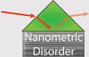
The research by the Team investigates a pile of nanometrically thin layers, that is, the thickness of each layer is approximately 20,000 times smaller than that of a sheet of paper. The precise thickness of the layers is deliberately taken to be random and normally such a nanometric disorder should not have any physical significance. However, this study demonstrates that an increase in thickness of a single layer to a mere 2 nm, or ~6 atoms, somewhere within the structure can be sensed if the structure is illuminated by light at a particular angle of incidence. In addition, the integrated impact of all the random deviations in all the layers leads to a highly significant physical phenomenon known as Anderson localization, although in a system where it was considered to have faint impacts.
This work demonstrates that light can be trapped in structures much thinner than the wavelength of light and that minute changes in this structure are observable. This makes the structure highly sensitive to the environment.
Professor Azriel Genack, City University of New York
Anderson was awarded the Nobel Prize in Physics in the year 1977 for discovering electron localization in the year 1958. Electron localization is the phenomenon in which a system is changed from being a conductor to being an insulator as a result of a disorder. Demonstrated to be a general wave phenomenon, it is applicable not only to sound and light but also to electrons. It is highly challenging to demonstrate Anderson localization in the lab. In general, localization has essentially no impact when random matters of a sample are considerably smaller than the optical wavelength. Actually, the random arrangement of atoms in a disordered medium (e.g. glass) cannot be observed by using visible light—the glass seems absolutely homogeneous even when viewed through the finest optical microscope. Yet, the localization effect observed in this latest study is astonishingly robust.
Considering a rough equivalent to the physics behind these outcomes, try conversing with a person in the same room that has a loud engine. One way to make the person hear your voice is to increase your voice above the engine’s sound. However, you can also speak by finding a silent spot in the noise at which the sound of the engine is comparatively weak. The sound of the engine is equivalent to the 'average' impact of the layers, and increasing one’s voice is similar to inducing a 'strong' disorder with wavelength-sized components. Yet, this study has shown that such structures present an 'exceptional point' analogue to the silent spot in the room — a point in which, even if the disorder is weak (i.e. nanometric), the average effect of the structure is more weak. Therefore, the parts of the study carried out adjacent to this point show an increased sensitivity to disorder and exhibit Anderson localization.
The outcomes of the research are a proof-of-concept that might open the door for vital, innovative applications in sensing. This method may allow the use of optical techniques to make high-speed measurements of nanometric defects in photonic devices and computer chips.