Jul 24 2007
A key discovery at Rensselaer Polytechnic Institute could help advance the role of graphene as a possible heir to copper and silicon in nanoelectronics.
Graphene, a one-atom-thick sheet of carbon, eluded scientists for years but was finally made in the laboratory in 2004 with the help of everyday, store-bought clear adhesive tape. Graphite, the common material used in most pencils, is made up of countless layers of graphene. Researchers simply used the gentle stickiness of tape to break apart these layers.
 A representation of conduction channels on a graphene nanoribbon interfaced with gold contacts.
Saroj Nayak, an associate professor in Rensselaer’s Department of Physics, Applied Physics and Astronomy, has worked with graduate student Philip Shemella and others for two years to determine how graphene’s extremely efficient conductive properties can be exploited for use in nanoelectronics. After running dozens of robust computer simulations, the group has demonstrated for the first time that the length, as well as the width, of graphene directly impacts the material’s conduction properties.
Nayak, Shemella, and their team outlined their findings in the report “Energy Gaps in Zero-Dimensional Graphene Nanoribbons” published in the July 23 issue of Applied Physics Letters.
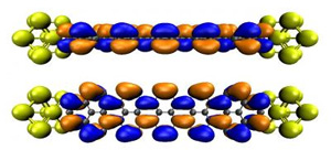
In the form of a long 1-D nanoscale ribbon, which looks like molecular chicken wire, graphene demonstrates unique electrical properties that include either metallic or semiconducting behavior. When short segments of this ribbon are isolated into tiny zero-dimensional (0-D) segments called “nanorectangles,” where the width is measured in atoms, they are classified as either “armchair” or “zigzag” graphene nanoribbons. Both types of nanorectangles have unique and fascinating properties.
Nayak, Shemella and the group took 1-D nanoribbons and trimmed the length down to a few nanometers, so the length was only a few times greater than the width. The lengths of the resulting zero-dimensional graphene nanorectangles had clear and distinct effects on the material’s properties.
The team used quantum mechanical simulations with predictive capability to carry out this work. Their computational study showed for the first time that the length of graphene may be used to manipulate and tune the material’s energy gap. This is important because energy gaps determine if the graphene is metallic or semiconducting.
Generally, when graphene is synthesized, there is a mix of metallic and semiconductor materials. But Nayak’s findings give researchers a blueprint that should allow them to purposefully make entire batches of either one or the other.
This research is an important first step, Nayak and Shemella said, for developing a way to mass produce metallic graphene that could one day replace copper as the primary interconnect material on nearly all computer chips.
The size of computer chips has shrunk dramatically over the past decade, but has recently hit a bottleneck, Nayak said. As copper interconnects get smaller, the copper’s resistance increases and its ability to conduct electricity degrades. This means fewer electrons are able to pass through the copper successfully, and any lingering electrons are expressed as heat. This heat can have negative effects on both a computer chip’s speed and performance.
Researchers in both industry and academia are looking for alternative materials to replace copper as interconnects. Graphene could be a possible successor to copper, Nayak said, because of metallic graphene’s excellent conductivity. Even at room temperature, electrons pass effortlessly, near the speed of light and with little resistance, through metallic graphene. This would almost ensure a graphene interconnect would stay much cooler than a copper interconnect of the same size.
It will likely be years before a graphene interconnect is realized, but major computer companies including IBM and Intel have taken notice of the material. Nayak said graphene is also currently a “hot topic” in academia.
Carbon nanotubes, which are essentially made of rolled-up graphene, are another potential heir to replace copper as the primary material used for interconnects. But they suffer from setbacks similar to those of graphene, Nayak said. When single-walled carbon nanotubes are synthesized, about one-third of the batch is metallic and the remaining two-thirds are semiconductors. It would be extremely difficult to separate the two on a mass scale, Nayak said. On the contrary, recent research at Rensselaer and elsewhere shows graphene could be produced in a more controlled way.
“Fundamentally, at this point, graphene shows much potential for use in interconnects as well as transistors,” Nayak said.
It is also possible that semiconductor graphene could one day be used in place of silicon as the primary semiconductor used in all computer chips, but research into this possibility is still extremely preliminary, Nayak said.