Dec 13 2007
The National Institute of Standards and Technology (NIST) has developed an imaging system that quickly maps the mechanical properties of materials - how stiff or stretchy they are, for example - at scales on the order of billionths of a meter. The new tool can be a cost-effective way to design and characterize mixed nanoscale materials such as composites or thin-film structures.
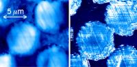 An atomic force microscope normally reveals the topography of a composite material (l.) NIST's new apparatus adds software and electronics to map nanomechanical properties (r.) The NIST system reveals that the glass fibers are stiffer than the surrounding polymer matrix but sometimes soften at their cores.
The NIST nanomechanical mapper uses custom software and electronics to process data acquired by a conventional atomic force microscope (AFM), transforming the microscope’s normal topographical maps of surfaces into precise two-dimensional representations of mechanical properties near the surface. The images enable scientists to see variations in elasticity, adhesion or friction, which may vary in different materials even after they are mixed together. The NIST system, described fully for the first time in a new paper, can make an image in minutes whereas competing systems might take an entire day.
The images are based on measurements and interpretations of changes in frequency as a vibrating AFM tip scans a surface. Such measurements have commonly been made at stationary positions, but until now 2D imaging at many points across a sample has been too slow to be practical. The NIST DSP-RTS system (for digital signal processor-based resonance tracking system) has the special feature of locking onto and tracking changes in frequency as the tip moves over a surface. Mechanical properties of a sample are deduced from calculations based on measurements of the vibrational frequencies of the AFM tip in the air and changes in frequency when the tip contacts the material surface.
NIST materials researchers have used the system to map elastic properties of thin films with finer spatial resolution than is possible with other tools. The DSP-RTS can produce a 256 × 256 pixel image with micrometer-scale dimensions in 20 to 25 minutes. The new system also is modular and offers greater flexibility than competing approaches. Adding capability to map additional materials properties can be as simple as updating the software.