Dec 18 2008
AMD, IBM and its Fishkill Alliance partners, Intel, an NEC-Toshiba collaborative effort and TSMC all presented leading-edge logic processes at 45, 32 and 22 nm design rules at the International Electron Devices Meeting (IEDM). Although several of the processes are not expected to go into production in the form presented this week, Intel said during a late paper presentation that it has completed the process development phase of its 32 nm process.
An all-star cast of companies presented leading-edge processes yesterday at a session on advanced CMOS logic at the International Electron Devices Meeting (IEDM) in San Francisco.
A presentation on 22 nm technology from a team based at Albany NanoTech (Albany, N.Y.) - including Advanced Micro Devices Inc. (AMD, Sunnyvale, Calif.), IBM Research (Yorktown Heights, N.Y.) and Freescale Semiconductor Inc. (Austin, Texas) - detailed the challenges facing leading-edge CMOS.
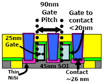
In the session's opening presentation on a 22 nm SRAM, IBM researcher B.S. Haran said for 22 nm logic "there is no space left. It is such a tight pitch, it is difficult to find a place to land the contact, and a thick spacer is no longer a luxury we can afford. The spacer, gate length and contact all must be scaled."
IBM used a double exposure/double etch process to scale the contacts.
To scale the contact pitch to 26 nm, IBM used a split mask approach with double exposure/double etch (DE2) steps. The 0.1 µm2 SRAM bit cell measures 0.554 µm (H) and 0.18 µm (W), with a contact that scales from 70 nm at the top to 26 nm at the bottom. "Getting down to the right CDs at the bottom of the contacts involved using aggressive chemical shrinks," Haran said, combining etch steps with the use of immersion patterning.
Although printing the contacts was a major challenge, the team also faced hurdles in creating the small vias. "If we used conventional tungsten, it would be full of voids, so we used copper," Haran said. "There are two concerns with copper vias: People are very concerned about poisoning from copper, and because the back end is near its limits for PVD copper, we had to use advanced liners to get a void-free film."
Taiwan Semiconductor Manufacturing Co. Ltd. (TSMC, Hsinchu, Taiwan) described its 32 nm technology, aimed at what R&D manager Carlos Diaz said was "high performance at low-power" applications.
Diaz opened his presentation by saying that, although TSMC could have introduced a high-k/metal gate technology at 32 nm, it decided to use high-k at the 28 nm node instead for customers needing it. The 32 nm IEDM presentation included a high-k/metal gate module with a 0.9 nm effective oxide thickness (EOT), but that technology will see production only at 28 nm design rules.
"The gate-first metal gate/high-k technology enabled us to scale the transistor; it allowed us to eliminate gate length," Diaz said. The transistor has a 30 nm physical gate length and a 130 nm gate pitch. He said the drive currents of 1340/940 µA/µm at an off current of 100 nA/µm "are the highest drive currents reported for a gate-first process." That was an apparent dig at IBM, which also uses a gate-first high-k/metal gate process.
During the question-and-answer session, Diaz said significant improvements to line edge roughness (LER) in the patterning steps allowed TSMC to reduce transistor mismatch, or threshold voltage variability.
Franck Arnaud, an STMicroelectronics manager assigned to the IBM Fishkill Alliance, described a 32 nm bulk technology that he said was aimed at networking, graphics and PC peripherals that require high data rates. He said the goal was to develop "the simplest, most cost-effective process possible that could be scaled to 28 nm quickly."
The general-purpose process builds on a low-power 32 nm transistor, adding embedded SiGe to the PMOS transistor to boost the drive current to 1050/650 µA/µm at an off current of 10 nA, which Arnaud said was "a dramatic drive current improvement with respect to published foundry data using SiON" as the gate dielectric.
Intel Corp. (Santa Clara, Calif.) presented its 45 nm system-on-a-chip (SoC) process, a new flow that includes support for analog, RF and other functions needed for communications-capable devices. Chia-Hong Jan, SoC process development manager at Intel, said the defining goal for the 45 nm SoC process was to build on Intel's processor-centric 45 nm technology and reduce the leakage current by 100×, achieving a 1 nA/ µm goal. The addition of high-k/metal gate at the 45 nm generation allowed Intel to achieve a 60% performance improvement compared with Intel's 65 nm low-power transistor, Jan said, adding that high-k reduced the poly depletion seen at 65 nm and allowed improved stress components.
Kirklen Henson presented an IBM paper on a silicon-on-insulator (SOI) process at 45 nm design rules with a gate-first high-k/metal gate flow. After the presentation, Henson said IBM will not put the 45 nm high-k process into production, but will accelerate introduction of the 32 nm SOI process, expected to come next year.
"At the end of the day, we were striving for high drive currents at a fixed Ioff. We could get higher drive currents with scaled gate lengths, but you certainly don't want higher power," he said. IBM achieved a 25 nm gate length with "very nice control of short channel effects," he said, adding that the industry is "up against a wall. We must control short channel effects, but if you are not careful you can scale the gate length and lose control of the channel."
The technology delivered a 25% performance improvement, which Henson said was a combination of drive current measurements, ring oscillator speeds and other metrics.
Jan Hoentschel, representing a team based at AMD Dresden, described an asymmetric transistor, which alters the doping profile by tilting the implant steps, creating asymmetric halos and a steeper junction profile. The approach requires four additional mask steps and care must be taken to avoid implant blocking.
Hoentschel said the approach delivered 9-12% product-level speed improvements, and a 12% ring oscillator boost. At the post-session author interview period, he said it remains undecided whether AMD product groups will use the process.
A combined NEC-Toshiba team presented two papers - one on a 40 nm low-power CMOS, and another on a 32 nm project that incorporated a hafnium-doped gate dielectric. However, Toshiba is a member of the IBM Fishkill Alliance, and NEC joined the IBM-led alliance several months ago, making it unclear if the jointly developed NEC-Toshiba technology will ever be brought into fabs. Shunsuke Hasegawa, the Toshiba engineer who presented the 32 nm paper, said Toshiba is committed to using the Fishkill-developed process at its logic fabs. When asked about the NEC-Toshiba processes, he said the companies are still discussing the matter.
A Toshiba spokesman said the joint NEC-Toshiba process "is still in the integration stage and we have not decided, as yet, if this solution is to be applied to mass production or not, though it is one of the candidates."
The final late paper in the session came from Intel 32 nm program manager Sanjay Natarajan, who said the 32 nm process achieves a doubling in SRAM density, with 4.2 Mb/mm2 achieved for the 32 nm technology. "This 2× density keeps Intel on the trend line for four generations," scaling the linear dimensions by 0.7× every two years.
He rebuffed critics who have argued that high-k/metal gate steps are expensive and detract from yields. Intel claims that high-k/metal gate added 4% to process costs at the 45 nm node, and Natar