Jan 5 2009
Scientists in Sweden have discovered new ways to control the growth and structure of nanowires at the single-atom level. Their findings, which provide major insights into materials physics, have come out of the NODE (' Nanowire-based one-dimensional electronics') project, funded with approximately EUR 9.5 million under the EU's Sixth Framework Programme (FP6). The study is published in the January issue of Nature Nanotechnology.
Nanowires, also known as 'quantum wires,' are single strips of atoms that are produced only in laboratories. Among other things, semiconductor nanowires show promise for nanoelectronics, as they might be used to link miniscule components within extremely small circuits in a 'molecular computer'.
Most semiconductor materials used to make nanowires develop irregularities and faults as they grow. These defects have a negative impact on the material's electronic and optical properties. In this latest research, scientists used Indium Arsenide (InAs), a valuable material in nanoelectonics, electron transport and spintronics, to determine how the structure of nanowires could be more carefully controlled.
'Two of the key parameters needed to control the crystal structure are nanowire diameter and the temperature at which they are fabricated,' explained co-author Kimberly Dick at Lund University in Sweden. 'But there are in total at least 10 to 12 different parameters that must be controlled when producing the nanowires.'
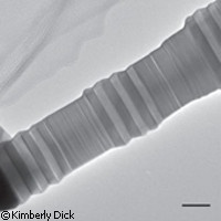
The researchers grew nanowires typically 10 to 100 nanometres in diameter and a few micrometers long. They did this by 'baking' the material in its gas form, using microscopic gold 'seeds' to start the wire. The diameter of the wire was controlled by changing the size of the seed. They successfully demonstrated that it is possible to control the growth of the nanowires, thereby drastically reducing irregularities.
In addition, they created different crystal structures of the same material by varying the temperature between 400ºC and 480ºC. By selectively tuning the crystal structure of InAs, they were able to consistently fabricate very strong 'superlattices' within single nanowires.
The scientists showed that it is possible to fabricate defect-free nanowires, and that one may alternate between different crystal structures along the length of a single nanowire. The new techniques, which the authors believe can be applied to other semiconductor materials, open the door for researchers to develop new functions for nanowires.
The study provides experimental evidence for a theory that has been widely discussed. 'Although a diameter-dependent crystal structure has been proposed by many authors,' the study reads, 'this is the first time that such an effect has been experimentally demonstrated, with a high level of control.' Electron microscopy images show that the arrangement of atoms in the nanowire crystal exactly matches theoretical simulations.
According to Professor Lars Samuelson, also of Lund University, 'The results achieved here establish our position in this area of science and technology and give our ambitions an increased credibility.' The authors hope their findings may lead to developments in light-emission and solar cell applications.
Source: Cordis