Instrument Used
The OneView® IS from Gatan is both the highest performance and fastest fiber coupled CMOS camera, capable of capturing 16 MP images at up to 25 fps.
The STEMx™ system allows the speed of the scanning probe to be synchronized with the camera’s frame rate. This means that the collection of 4D STEM diffraction datasets can occur at full speed (up to 300 fps at 512 x 512 pixels).
Background
Within conventional 4D STEM technology, a central limiting factor is the speed at which diffraction images can be obtained at each pixel within the STEM image. This speed is primarily limited by both the speed at which 4D STEM datasets can be written and saved onto disk, and the frame rate of conventional CCD cameras (30 fps for 512 x 512 images).
These slow speeds can limit the amount of data that researchers are able to collect in a specific period. This means they are not feasible for beam sensitive specimens which may have limited allowable dose before they are damaged or structurally transformed.
Materials and Methods
Cross-section specimens that isolate specific ZnO nanowires (NW) were chosen for these experiments.
The growth direction of these nanowires, on a GaN substrate, can be guided as a function of substrate Ga-ion bombardment, which results in varied local surface boundaries to partition NW heterojunctions into separate segments and orientations.
HRTEM measurements had previously been used to ascertain the tolerance of crawling nanowires to lattice mismatch and strain. Conclusive quantitative strain measurements have been difficult to acquire due to the beam-sensitive nature of the specimen. The lack of a statistically sufficient number of diffraction measurements from the substrate-NW interface region also posed problems.
Using the OneView IS camera in conjunction with STEMx, two (256 x 85 x 1024 x 1024) datasets were collected, each in <2 min, from NWs grown on non-bombarded and bombarded substrates.
As well as the visual comparison of averaged diffraction patterns at different interface regions, 2D strain maps were calculated along orthogonal axes within the diffraction pattern, referencing the unstrained GaN substrate.
Making use of the STEMx Analytical Suite, the relative out-of-plane, in-plane, rotation and shear at the interface can be rapidly measured for sizable datasets (each >40 GB).
The current strain mapping results highlight the degree and character of lateral strain (ε_uu) is more relaxed in directions parallel to the nanowire long axis through the ion bombarded regions (Figure 1) compared to the localized intense lateral strain points perpendicular to the same axis (ε_uu in Figure 2).
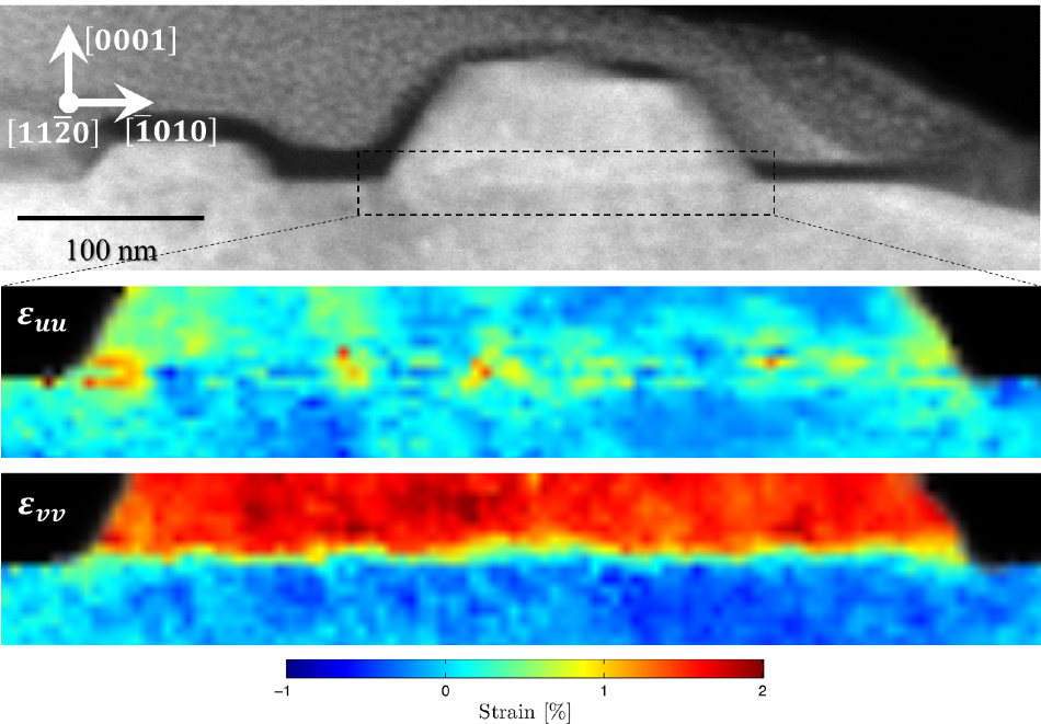
Figure 1. HAADF (top) of nanowire cross-section. Expanded view of CBED diffraction map taken over 256 x 85 pixel area corresponding to dotted outline and extracted using STEMx software shown below. Localized points of strain in the lateral (ε_uu) crystalline dimension and compressive strain (ε_vv) are shown below. Image Credit: Gatan.
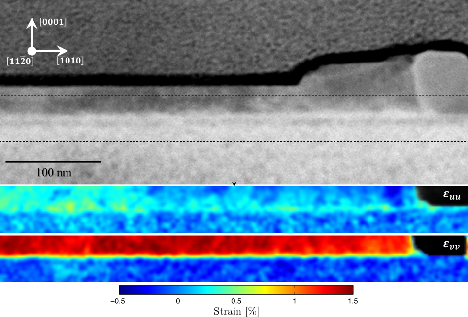
Figure 2. HAADF (top) of nanowire cross-section. Expanded view of CBED diffraction map taken over 256 x 85 pixel area corresponding to dotted outline and extracted using STEMx software shown below. Localized points of strain in the lateral (ε_uu) crystalline dimension and compressive strain (ε_vv) are shown below. mage Credit: Gatan.
The relative degree of compressive strain (ε_vv) was noted to be similar in either case.
The collection of additional data is required to support these conclusions. Current experiments have suggested new means of both controlling and comprehending the lateral epitaxy of nanocrystals.
These results can have wide-ranging implications; touching areas of the future fabrication of nanowire-based devices. For example, incorporating II-V and III-nitride semiconductors into existing industrial processes or combining top-down and bottom-up fabrication techniques.
Summary
By using the STEMx system, the fast frame rate OneView camera was employed to drive the STEM probe on beam sensitive ZnO NWs that were grown on GaN substrates. High-speed 4D STEM data acquisition substantially reduced the damage to specimens that had been encountered during previous data collection (saving time and money).
The data obtained with the OneView camera delivers high-resolution results, and is capable of direct observation of single systems over considerable length-scales. Using intelligent data modeling, it also allows for a visualization of nanoscale effects in an overall microsystem.
Results such as these produce valuable insight into the mechanisms of nano epitaxial growth, as well as offering foundational information on incorporating these systems into future technologies.
Credits
Special thanks to Dr. E. Garratt (NIST), Dr. A. Herzing (NIST), Dr. C. Ophus (NCEM) and Dr. J. Ciston (NCEM).

This information has been sourced, reviewed and adapted from materials provided by Gatan, Inc.
For more information on this source, please visit Gatan, Inc.