Feb 5 2010
The New Energy and Industrial Technology Development Organization (NEDO) and the National Institute of Advanced Industrial Science and Technology (AIST) announced that, as a part of Industrial Technology Research Grant Program, Takeshi Tanaka (Research Scientist) of AIST, and his colleagues have successfully developed a method for high-purity separation of single-walled carbon nanotubes (SWCNTs)* into metallic SWCNTs and semiconducting SWCNTs by using a column packed with agarose gel**.
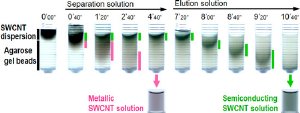 Separation of metallic and semiconducting SWCNTs in a column packed with agarose gel beads. When SWCNTs dispersed in a solution were applied to the column, reddish metallic SWCNTs passed through the gel (pink bar), while green semiconducting SWCNTs (green bar) were adsorbed onto the gel. The adsorbed semiconducting SWCNTs can be collected with the eluent. (The numerals indicate the time in minute' second".)
Since this method allows low-cost separation by automation of the separation process and by permitting reuse of the gel, industrial applications of separated metallic and semiconducting SWCNTs utilizing their characteristics are expected.
This result will be published today (Nov. 27) in Applied Physics Express (online version), which is published by the Japan Society of Applied Physics. It will also be exhibited in nano tech 2010, which will be held on February 17 to 19, 2010, at Tokyo Big Sight.
* A single-walled carbon nanotube is a tubular substance in which carbon atoms form hexagonal networks similar to that observed in graphite. The diameter of the tube is about 0.7–4 nm (1 nm = one billionth of a meter). The tube exhibits metallic or semiconducting properties according to the arrangement of hexagons.
** Agarose is a polysaccharide obtained from seaweed and is the principal ingredient of agar. Agarose gel is prepared by dissolving agarose in hot water and cooling the solution until it solidifies.
Summary
Takeshi Tanaka (Research Scientist) and Hiromichi Kataura (Leader), the Self-Assembled Nano-Electronics Group, the Nanotechnology Research Institute (Director: Nobutsugu Minami) of AIST (President: Tamotsu Nomakuchi), developed a method for high-purity separation of SWCNTs into metallic SWCNTs and semiconducting SWCNTs by using a column packed with agarose gel beads, as a part of Industrial Technology Research Grant Program of NEDO.
The synthesis of SWCNTs usually yields a 1:2 mixture of metallic and semiconducting SWCNTs. Although these two types of SWCNTs must be separated for their application in electrical devices, this separation cannot be achieved easily. AIST had developed methods for separating metallic and semiconducting SWCNTs by using agarose gel. AIST has subsequently improved these methods and achieved a low-cost high-purity separation method. This method involves the use of a column packed with agarose gel beads, in which the semiconducting SWCNTs are selectively adsorbed and then eluted (Fig. 1). The gel-packed column can be used repeatedly, and the separation process can be easily automated. This approach allows low-cost production of SWCNTs, thereby facilitating industrial production of metallic and semiconducting SWCNTs.