Attolight’s technology is based on a well-known phenomenon called cathodoluminescence (CL). CL refers to the light emitted by any material under electron irradiation. The best known CL application is former cathode ray tube-based television sets. CL becomes a very powerful defect inspection technique when implemented in a modern electron microscope (EM) that can perform rapid, non-destructive defect inspection on a full wafer scale. Even though CL has been known for a long time, technical implementations have been restricted to manual laboratory use.
Attolight’s Completely Integrated CL System Approach
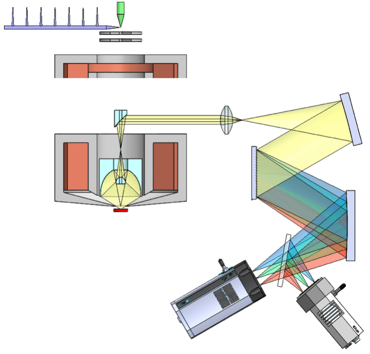
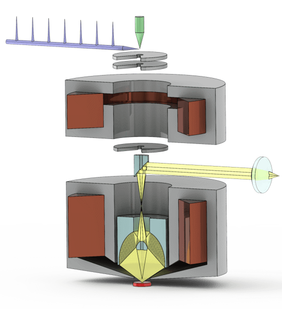
Attolight is considered to be the only provider of completely integrated cathodoluminescence (CL) systems: Attolight designs, builds, and then optimizes both light and electron optics in order to obtain high-efficiency CL collection while keeping the products simple to operate. Attolight’s CL systems have been designed for both R&D and industrial environments with outstanding performance that is achieved, thanks to proprietary and patented optical designs.
Typical competing solutions comprise of a light collection add-on that is mounted on a standard Scanning Electron Microscope (SEM). This approach leads to sub-optimal performance in terms of light collection efficiency and reproducibility. Furthermore, these systems need a dedicated operator who, in several cases, needs a solid scientific background in spectroscopy in order to correctly use the system. Finally, if the CL detection system is not performing up to specification, this could result from a problem in the CL detection system, the SEM, or in the detector alignment with the SEM. It can be tough to know (a) whether alignment alone is the issue, and (b) if there is a system problem, which manufacturer to call in for a repair.
Quantitative CL
Attolight’s light collection optics is designed in a way so that the light collection efficiency is continuous over a field of view (FOV) of 300 µm. This allows the user to quantitatively compare measured spectral shape, intensity and wavelength position in different regions of the field of view. Competing solutions use a different light collection system in the form of an elliptical or parabolic mirror. Those systems feature by design a field of view of a couple of micrometers in the center axes of the optics.
Hyperspectral CL
Hyperspectral of spectral imaging designates an improved CL mode that registered the complete emission spectrum in every pixel. This mode requires a highly efficient light collection system along with high speed electronics and sensitive cameras.
Attolight’s products define hyperspectral CL by the capacity of producing images with 1600 channels – or colors – per pixel. The technology offers millisecond hyperspectral CL maps with an acquisition time of one millisecond per pixel because of a high collection efficiency (NA=0.72), guaranteed zero photon-loss on apertures over a field of view of 300 µm, optimized control of the entire microscope – from the scanning coils to the camera – and an extremely robust software solution capable of handling the huge data acquisition rate without stuttering.
Ultrafast Point Detection
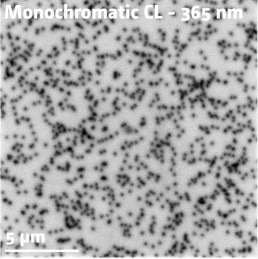
Ultrafast point detection (UPD) designates a CL detection mode in which an intensity at a given wavelength is recorded in every pixel. This mode is radically varies from hyperspectral mode (link) where full spectrum is registered in every single pixel.
UPD mode is often used for detecting defects that show up at a given wavelength or are non-radiative like the dislocations shown on the picture here.
UPD is about 100 times (about 1 minute for a hyperspectral map to below 1 s for a UPD map) faster than the hyperspectral mode which makes it extremely useful for several industrial applications where speed is key.
Pico-Second Time-Resolved CL
Attolight’s tool can be field-upgraded in order to measure pico-second luminescence decay times. Change from continuous to time-resolved mode can be performed on the fly with software control. This mode allows the measurement of minority carrier lifetimes and excited carrier diffusion distances. Standard time-resolved CL systems employ a beam blanker to “chop” the electron beam into short pulses. However, this approach leads to a loss in spatial resolution and time-resolution cannot reach the picosecond regime. This is the reason why Attolight employs a revolutionary technique in order to obtain short pulses: make use of the photoelectric effect by focalizing a short laser pulse on the electron emitter to cause photoelectron emission. By carefully synchronizing the ultrafast detector to the excitation laser, time-resolutions less than 10 ps can be attained. Attolight is considered to be the only company commercializing time-resolved CL systems based on this approach and has a global unique experience in implementing and employing such systems.
Short Time to Results
Sample alignment can be performed within seconds by any user, no prior spectroscopy experience is required. The alignment is performed with the emission signal the user wants to measure, yielding a perfect signal alignment. The readout of the light detection components is completely optimized in order to reach maximum measurement speeds. A hyperspectral map comprising of 40,000 pixels can be measured within just over 40 seconds. This means that a hypercube of data is developed containing intensity information on 1,600 colors per pixel, a complete optical characterization of the sample within seconds.
Proprietary Electron Gun Design to Yield Highest Current Densities
The Attolight CL tool’s proprietary electron optics are custom designed in such a way as to yield highest current densities for electron spot sizes less than 10 nm. It is possible to reach the following specifications:
- 30 nA for a spotsize below 10 nm
- 250 nA for a spotsize below 25 nm
As a result, the Attolight system can generate more CL signal for a given acceleration voltage compared to competing SEM-CL configurations or measure challenging materials such as silicon that emit extremely low levels of light.
Lowest Sample Stage Drift Low Temperature Stage
Attolight’s low temperature solution can effortlessly be added later as an upgrade without the requirement for changing the sample stage and the upgrade can be performed within hours. The Attolight cryostage solution shows very low drift, and, more importantly, no vibration measurable by the SEM. This is attained by mechanically de-coupling vibrations by using a copper braid and a flow-free solution.
Intuitive Touch-Screen Interface
Attolight’s tools are completely remote controlled by an intuitive user interface that is completely integrated on an iPad. This makes the tool easy to use and the user training very simple. All measurement data are registered on a server on the machine. It is possible to read data on any platform.
Data Analysis and Reporting Solution
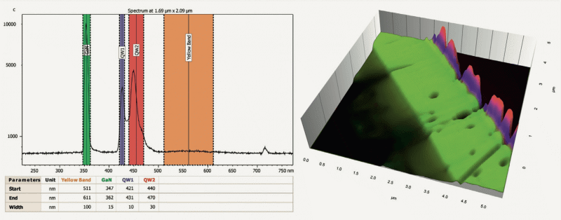
The Attolight CL microscope produces images comprising of up to 1,600 colors that are known as hyperspectral maps. AttoMap is considered to be Attolight’s powerful solution for visualizing hyperspectral maps as 2D RGB maps or 3D maps and producing visual data analysis reports. AttoMap is capable of optimizing the workflow and creating interactive, traceable reports. Furthermore, AttoMap permits the user to visualize 2D RGB maps and has a powerful feature to develop 3D maps. This feature is very helpful as it allows CL light intensity to be displayed in the third dimension, providing the user an extremely simple way of representing complex data.
The figure given below presents an example of a 3D map. Color bands are linked with relevant spectroscopic features. With the 3D image, emission intensity differences between features can be immediately recognized.
Electron Beam Induced Current (EBIC) Detection
The EBIC system (employed for obtaining high resolution electrical data on a sample) can be installed on initial installation or later as an upgrade. The EBIC module is completely compatible with the low temperature stage which can be important for specific types of samples. EBIC can be performed in parallel with CL, even at low temperature, thus both signals can be detected at the same time in exactly the same working conditions.

This information has been sourced, reviewed and adapted from materials provided by Attolight.
For more information on this source, please visit Attolight.