The emergence of new materials has opened the doors to nano-electronic and optoelectronic devices with new or improved capabilities. For example, III-V based alloys have transformed the LED industry seeking applications in high power electronics, and may accelerate micro-electronic devices in the near future. Unfortunately, the presence of highly concentrated crystallographic or impurity defects limit the wide scaled implementation of III-V based alloys. Since such defects are typically of sub-nanometric size, they cannot be easily observed directly. Defect metrology is by consequence of great significance to evaluate fabrication processes.
Traditional Methods and Drawbacks
Traditionally, three methods are used to establish the density of defects in optoelectronic devices.
- Transmission electron microscopy (TEM) is to date the most used technique. Despite being popular, it is very costly and has major disadvantages. The sample preparation is destructive, time-intensive and demands extensive training and skills. The image analysis is subject to interpretation and is not statistically relevant due to its ability to probe only small areas.
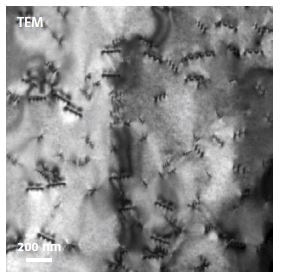
TEM image of a GaN sample exhibiting defects.
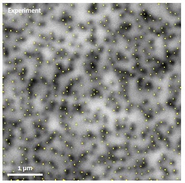
CL image of the same sample. Defects appear as dark spots. The yellow dots point the defects that are detected by the Attolight proprietary software.
- X-ray diffraction (XRD) is limited by the large size of the probe (50 µm) and can only probe an ensemble of defects. Furthermore, the technique is not adapted to low defect densities (where XRD’s sensitivity drops).
- Atomic force microscopy (AFM) is capable of scanning large areas with very good resolution. However, AFM measurements are usually time-intensive and can merely probe buried defects.
Advantages of Cathodoluminescence Microscope
On the other hand, cathodoluminescence (CL) microscope addresses these limitations by combining large field of view and small probe size. The Attolight CL microscope has unique features that make defect imaging and counting in optoelectronic devices more precise and cost effective.
- Its auto-aligned design and optimized light collection efficiency fasten defect density measurements down to a few minutes
- Its large field of view (300 µm) allows for examination of large areas while maintaining good spatial resolution. As a result, very low defect densities can be detected. Also, inhomogeneous distributions of defects can be observed directly.
- Its small probe size (<10 nm) provides for very good spatial resolution. The higher detectable defect densities are only limited by the diffusion length of carriers.
- Its unique touch-screen interface allows for user-friendly operation.
- It does not require sample preparation, making defect density measurements accessible to the non-specialist
- Attolight’s proprietary software allows quick and reliable automated defect counting
Defect density counting: Comparison of the Attolight CL microscope with TEM and AFM techniques
| |
TEM |
AFM |
Attolight CL |
| Sample 1 |
2.06 x 109 cm-2 |
|
2.07 x 109 cm-2 |
| Sample 2 |
|
2.90 x 108 cm-2 |
2.51 x 108 cm-2 |

This information has been sourced, reviewed and adapted from materials provided by Attolight.
For more information on this source, please visit Attolight.