Photolithography is an essential microfabrication technique used to pattern substrates for modern electronics, sensors and microfluidics. It is a precision form of customized surface fabrication where the interface of a wafer is coated with a photoresist, which is a light-sensitive polymer.
The coated wafer is then subjected to light exposure which is selectively attenuated by a mask, producing a latent image that is chemically, physically or optically etched to generate a permanent micro-structured pattern on the surface of the wafer.
Paired with metal deposition and etching techniques, photolithography is a dynamic method for microstructure production for chemical and bio-sensors, optics and microfluidic devices.
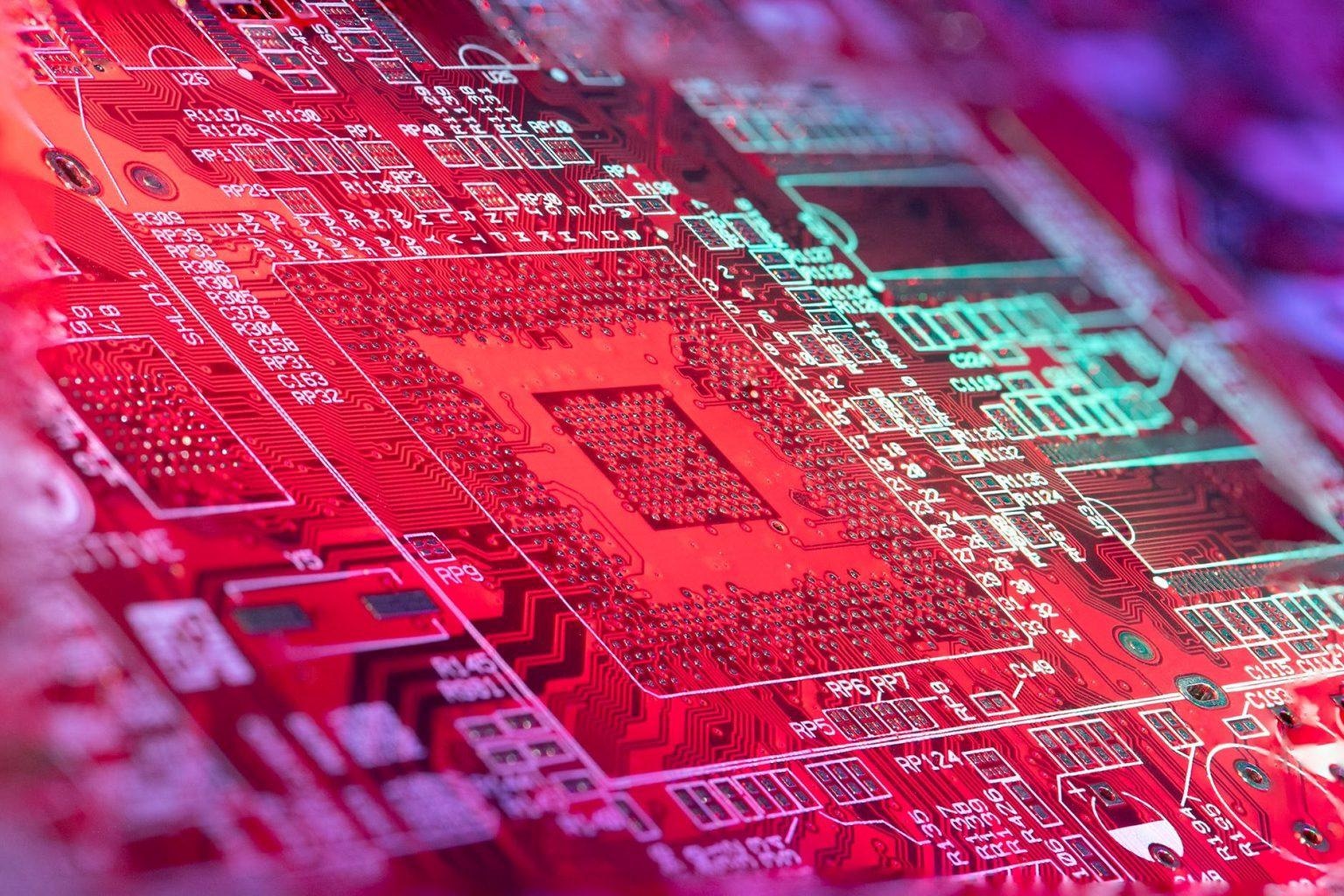
Image Credit: Nic Wood on Pexels.com
Understanding Photolithography
Moore’s law indicates that dense integrated circuits (ICs) double the number of on-chip transistors every two years.
Given that today’s photolithography techniques give manufacturers the ability to develop ICs with feature resolutions as low as a single micrometer (µm), it is only natural for printed electronics developments to decelerate or advance to the point of nanoscale processing.
Nanotechnology is pushing the boundaries of microfabrication, but engineers still have some way to go to reveal the true potential of what can be achieved at the microscale.
Photolithography has a major role to play in pushing the lithographic letter, particularly techniques such as i-line exposure with ultraviolet (UV) wavelengths — typically 365 nm.
In addition, photolithography service providers have the capacity to offer great expertise with complex epoxy and metal lift-off resists — an essential requirement for microscale surface fabrication.
All this facilitates photolithography solutions that grant engineers and scientists the power to achieve new levels of surface resolution and precision.
Applications of Photolithography
Patterned Gold Electrodes
Photolithography is a crucial element in the production of patterned gold electrodes, which gain advantage from high topographical uniformity and lateral precision, plus the intrinsic conductivity of gold, to yield high-performance electrical elements for state-of-the-art analytical applications and sensor development.
When developing patterned gold electrodes, one of the major development areas for patterned gold electrodes includes novel biosensors comprised of sophisticated microelectromechanical systems (MEMS) – or bioMEMS.
Optical Filters
Interference filters are application critical elements in photolithographic workflows, specifically in aftermarket i-line systems that necessitate the accurate resolution of a stable monochromatic light source.
Photolithography also takes a central role in generating OEM filters with selective, high-resolution surface patterns.
Moreover, pristine gold substrates are usually prepared for use in optical microscopy and state-of-the-art imaging techniques such as surface plasmon resonance (SPR).
Microwells and Micropillar Arrays
Biological and cellular imaging frequently employs microwell arrays made up of patterned substrates that facilitate an extensive range of functionalities for life science applications. For instance, honeycomb arrays generated via a photolithographic process are useful for stabilizing liquid films for particle separations.
Photolithography Services from Platypus Technologies
Platypus Tech understands how precious time and money are when working with highly parallel workflows such as substrate patterning.
Yet, the need for high-precision custom surfaces typically places the responsibility on end-users to come up with a solution that transcends the capacities of readily-available solutions.
That is why Platypus has developed a genuinely customizable photolithography service to meet the requirements of users across a range of research and development (R&D) areas.
Contact Platypus Tech today to find out more.

This information has been sourced, reviewed and adapted from materials provided by Platypus Technologies, LLC.
For more information on this source, please visit Platypus Technologies, LLC.