Many life sciences applications utilize photolithography, a technique for microfabricating materials, because it is a low-cost and efficient process. A substrate is covered with a photoresist and subjected to light to eliminate particular regions, leaving behind a patterned image.
This article discusses why photolithography is utilized to form patterns on metal surfaces and the benefits it delivers.
What is Photolithography?
Photolithography is a microfabrication method that creates intricate patterns on a material’s surface, also called patterning or optical lithography.
It is frequently used in microprocessor manufacturing and printed circuit boards (PCB), using a thin photosensitive polymer film (a positive photoresist) and etching the pattern with a UV light wavelength.
This process of patterning is straightforward but vital for its applications. The first step is the addition of the photoresist onto a substrate’s surface. A mask is subsequently placed over the photoresist and exposed to UV light.
This leaves a specific pattern on the polymer. After creating the pattern, the photoresist may be dissolved to access the substrate below.
Why Use Photolithography to Pattern Metal Surfaces?
The microfabrication method of photolithography enables the development of patterned thin films on the surface of a substrate, which forms a protective layer when the substrate undergoes processing methods.
Photolithography can only be performed on completely flat surfaces like silicon and base metals such as copper and aluminum.
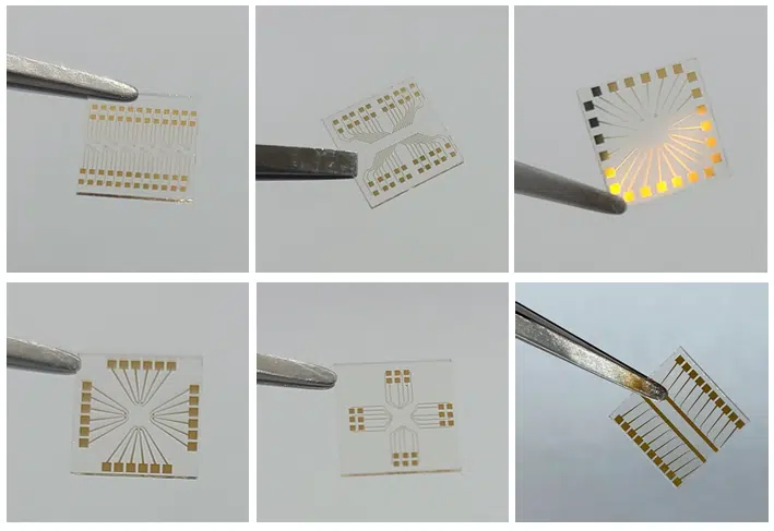
Photographs of gold thin-film electrodes on glass substrates. Image Credit: Platypus Technologies, LLC
Producing patterns on the metal’s surface can be carried out precisely using photolithography, enabling tight control over the process at a reasonable cost. The patterns generated with photolithography may be as small as a few tens of nanometers, allowing highly intricate details to be etched into the substrate.
Other advantages of employing photolithography for patterning metal surfaces include:
- Cost-effectiveness
- High levels of control over the process
- A fast and efficient process
- Excellent repeatability
- Suitable for a variety of flat-surfaced materials
- Utilized in various electronics applications, such as internal computer parts and biosensors
Photolithography plays a fundamental part in modern electronics since it is utilized for the creation of silicon wafers for semiconductor devices, microstructures for optics, integrated circuits, biosensors, and many more products.
Photolithography with Platypus Technologies
Platypus Technologies provides various metal coating services for a range of applications. One such service is photolithography, frequently employed for biosensor chips and gold films of various substrates.
Photolithography provides many benefits, from low cost to repeatability, but it is challenging for some laboratories to achieve as it requires an ultra-clean environment. Platypus Technologies can help with this, as it offers this service in a Class 100 cleanroom, ensuring high-quality surface patterning and outstanding repeatability.
If your application requires surface patterning, contact Platypus Technologies today for more information about its photolithography processes and services.
References and Further Reading
- https://www.news-medical.net/life-sciences/Photolithography-Microfabrication-Technique.aspx

This information has been sourced, reviewed and adapted from materials provided by Platypus Technologies, LLC.
For more information on this source, please visit Platypus Technologies, LLC.