The advanced nanoIR3-s from Bruker combines nanoscale IR spectroscopy (AFM-IR) and scattering scanning near-field optical microscopy (s-SNOM) with an integrated atomic force microscope (AFM), all in a single system.
The nanoIR3-s system is based on the legacy of Anasys technology leadership in AFM-based nano-optical characterization. It offers nanoscale IR spectroscopy, optical property mapping, and chemical imaging with a spatial resolution of 10 nm, as evidenced on 2D material samples.
In addition, the nanoIR3-s system allows AFM topographic imaging as well as AFM material property mapping, with nanometer-scale resolution. These capabilities make it the instrument of choice for correlative studies across various material science applications.
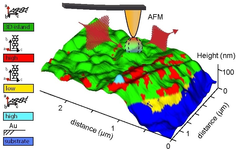
Correlative analysis of spatial map reconstructed from separate correlated AFM and chemical measurements reveal molecular orientation of vacuum-deposited PTCDA defects. Science Advances 2 (10), e1601006 - E. A. Muller, et al.
Features of the nanoIR3-s System
- High-resolution, fully featured AFM with thermal, mechanical, and electrical modes
- Complementary AFM-IR and s-SNOM techniques
- Femtosecond broadband nano-FTIR spectroscopy
Complementary Nanoscale Techniques
s-SNOM
The near-field phase and amplitude of the scattered light are determined using patented methods for s-SNOM. This can be achieved as the probe scans over the surface of the sample to produce near-field optical images concurrent with the topography image.
Alternatively, the probe can be placed at a fixed place and the source’s wavelength can be altered to provide near-field spectra. As a patented capability, POINTspectra offers both spectroscopy and chemical imaging for CW QCL laser operation.
Tapping AFM-IR
The same photothermal detection mechanism is used by Tapping AFM-IR as resonance-enhanced AFM-IR; however, Tapping AFM mode operation is used as the sensing mechanism. Additionally, an exclusively designed Tapping AFM-IR probe is driven at varied harmonic resonances/modes to detect photothermal expansion.
With Tapping AFM-IR, lower AFM probes forces are applied to the sample to achieve higher spatial resolution chemical imaging to 10 nm or below, depending on the type of sample.
Resonance-Enhanced AFM-IR
Within the instrument, the resonance-enhanced AFM-IR component works by illuminating the sample in a top-down fashion with a tunable, broadband, pulsed mid-IR laser. The sample selectively absorbs the pulsed radiation. This results in rapid and transient local expansion, which is detected by the resulting mechanical deflection of the AFM probe.
The IR absorbance spectra, thus obtained, can be directly associated with FT-IR absorbance spectra, enabling seamless interpretation. The IR absorbance spectra can be searched against available IR spectral database libraries.
Mechanical Property Mapping, NanoThermal Analysis, and Electrical AFM Modes
Apart from nanoscale IR spectroscopy, the nanoIR3-s system is capable of measuring contact resonance frequencies of an AFM cantilever using the Lorentz Contact Resonance technique (LCR). This helps in mapping the differences in the mechanical characteristics of a sample.
In addition, the nanoTA technique can be used for imaging local thermal characteristics to make quantitative measurements of thermal transition temperatures at nanoscale spatial resolution.
 Download: Chemical Characterization of Polymeric Films, Blends, and Self-Assembled Monomers
| Modes |
| Chemical Imaging Modes |
Tapping AFM-IR; FASTspectra (AFM-IR); FASTmapping (AFM-IR); Hyperspectral Imaging; s-SNOM |
| AFM Modes |
Standard: tapping; contact phase; force calibration; lateral force; EFM/MFM Optional: NanoTA; SThM; LCR; C-AFM; KPFM |
| Key Laser Options |
| POINTspectra QCL Laser |
6 or 4 chip continuous wave/pulsed with 950-1900 cm-1 range for s-SNOM and AFM-IR, additional wavelengths available upon request |
| Single/Multiple Chip QCL Laser |
Single or multi-chip continuous wave/pulsed with different spectral ranges for s-SNOM |
| CO2 Laser |
For use with s-SNOM |
Visible 632.8 nm
HeNe Laser |
10 mw and optics package for integration into nanoIR3-s |
| 1550 nm NIR Diode Laser |
5 mw and optics package for integration into nanoIR3-s |
| AFM Performance |
| Z Noise |
<100 pm RMS |
| XY Scan Range |
50 µm x 50 µm |
| Z Range |
>4 µm |
| Scan Resolution |
≤1024 x 1024 pixels |
| XY Scan Stage |
Flexure with capacitive closed-loop sensing |
| Tip Positioning Accuracy |
±10 nm |
| Sample Size and Movement |
| Sample Size |
<25 mm dia max |
| Sample height |
<10 mm max |
| XY Stage Range |
8 x 8 mm motorized |
| Z stage Range |
>5 mm motorized |
| Optical Microscopes |
| Illumination |
Brightfield |
| CCD Resolution |
1.5 µm 5 MP |
| Digital Zoom |
3X |
| Objective |
10X |
| Field of view |
~900 x 600 µm max; ~450 x 300 µm min |
Download the full datasheet for the Anasys nanoIR3-s.