Electro Scientific Industries (Nasdaq: ESIO), a leading supplier of innovative, laser-based manufacturing solutions for the microtechnology industry, today unveiled its new 9900 system for ultra-thin wafer dicing.
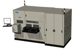 9900 system
Announced at the SEMICON West 2010 tradeshow in San Francisco, ESI’s fully automated 9900 system delivers unparalleled die break strength (DBS) with a proprietary, highly efficient, laser-based architecture for rapidly dicing ultra-thin silicon wafers (<50 microns).
“As higher levels of functionality are being incorporated into portable electronic devices, the wafers required for advanced packaging and 3D integration applications are getting thinner and thinner,” said Nick Konidaris, president and CEO of ESI. “Our customers are pushing the current limits of traditional wafer dicing equipment and are demanding advanced technologies to improve yields and total cost of ownership.”
Breakthrough technology for advancing market needs
Miniaturization and convergence are driving a significant increase in 3D packaging technology. Semiconductor Equipment and Materials International (SEMI®) reports that 3D integration is anticipated to be pivotal for future growth of the semiconductor industry.1 Ultra-thin wafers are required to support the advancements in 3D packaging, such as:
- Stacked memory for high density storage applications
- System in package (SiP) that combines stacked logic and memory
- Through silicon via (TSV) interconnect applications
There are challenges with using mechanical technology for dicing ultra-thin wafers due to cracking, chipping, and other yield and quality issues. ESI’s 9900 is the first production-ready, fully automated wafer dicing system that uses its proprietary laser-based architecture to quickly and efficiently cut ultra-thin wafers. The 9900 reliably yields die that can withstand the rigors of advanced packaging requirements.
“The 9900 is revolutionary for the semiconductor industry as it will enable our customers to fully adopt 3D integration into their high volume manufacturing environments,” said Louis Vintro, vice president and general manager of ESI’s Semiconductor Products Division. “By combining ESI's proprietary processing technology with our world-class systems expertise, we are delivering the first production-worthy ultra-thin wafer dicing solution.”
Optimized for high precision and speed, the innovative features and benefits delivered by the 9900 include:
- Advanced technology in one integrated system – The 9900 enables full-cut dicing of ultra-thin wafers and scribing logic or system on chip (SoC) wafers on die attach films (DAFs) in one integrated system.
- Unparalleled die break strength – Some wafers have delicate, brittle, low k materials on the topmost layers of the wafer. Cutting through this without damage is critical. The 9900 uses a proprietary laser and dry etch process to maximize die strength for the most challenging applications.
- Increased precision and yields – The 9900 uses a precision-controlled laser with 355nm wavelength output to the ultra-thin wafer surface. This enables manufacturers to minimize scribe line widths and produce more die per wafer.
- Optimized run rates – The easy-to-use software and recipe library allow customers to optimize run rates for their specific manufacturing applications.
Source: http://www.esi.com/