Eulitha AG, a Swiss based nanolithography company, has developed a proprietary photolithography technology for low-cost and high-throughput fabrication of photonic nanostructures. This solves a major ongoing problem faced in the fabrication of high-resolution photonic structures since standard photolithography equipment either lacks the required resolution or its cost is prohibitively high.
The patented technology enables the formation of periodic nanostructures over large areas for such applications as LEDs, solar cells and flat-screen displays.
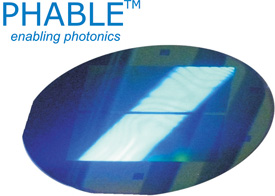
The new technology, dubbed PHABLE (for Photonics Enabler), is a mask based UV lithography. Unlike currently available technologies, the PHABLE system forms an image that has practically unlimited depth of focus. Therefore non-flat substrates, such as LED wafers, can be patterned uniformly and reproducibly. It also allows combinations of different patterns such as linear diffraction gratings and arrays of holes on hexagonal or square grids to be printed using a single exposure onto a chip or a wafer. The resolution of the printed features can be as small as one quarter of the illumination wavelength. The masks required by PHABLE can be produced inexpensively using standard chromium-on-quartz mask-writing technology. The technology will be presented at the MNC 2010 conference in Fukuoka, Japan, between November 9-12, 2010.
Photonic crystals needed for enhancing the light extraction efficiency of LEDs is one of the major applications of the new technology. Unlike the Nanoimprint method that is commonly employed for this purpose, it avoids contact between the mask and the wafer, and it does not require consumable soft-stamps. Therefore an expensive two-step process is avoided. It is expected that other applications will also benefit greatly from this development, including nanowire-based LEDs and photovoltaic devices, heteroepitaxy on patterned silicon substrates and epitaxial lateral overgrowth (ELO) used in blue-ray lasers. Wire-grid polarizers, as required for both LCD displays and projectors, may also be produced with the PHABLE technology.
The compatibility of PHABLE with conventional masks and UV- exposure processing will ensure a smooth adoption of PHABLE by the industry. Standard photoresists with suitable resolution and etch properties are available from multiple vendors. Therefore, HB-LED and other device manufacturers will be able to rely on the usual, well-established sources for obtaining the required consumable materials so as to ensure a low-cost manufacturing process for their photonic nanostructures.
Eulitha now offers samples and wafer batch processing services to companies and researchers developing nanostructure-based products who are interested in taking advantage of this breakthrough technology. It is also currently offering laboratory lithography tools for 2”-4” wafers that are suitable for product development. High-volume production tools with throughput in excess of 100 wafer-per-hour will be made available to manufacturers in the near future. Eulitha expects many future photonic devices to shine even brighter with the introduction of the PHABLE technology.