In May of 2013, Nanotronics Imaging installed an nSPEC® at Kyma Technologies in Raleigh, North Carolina. The companies have quickly established a collaborative partnership after initially meeting in early 2013. The nSPEC® enables Kyma to inspect their wafers via powerful image analysis software. This includes the ability to store high resolution images, capture particular features and areas of interest while translating the acquired visual information into quantifiable data.
Keith Evans, President and CEO at Kyma, states “We are very pleased with the kinds of inspection that the nSPEC® is giving us, which has already given us significant new insight into our processes here at Kyma.”
Kyma Technologies has graciously agreed to open their doors for people to observe the nSPEC® in action. This is an ideal opportunity for semiconductor groups and Universities in the South Eastern region of the U.S. to learn about the powerful capabilities of nSPEC® and its value to their respective applications. “This is really a great partnership and opportunity for us, we are so thrilled that Kyma is happy with their purchase of an nSPEC® and are excited to bring interested people and future partners to Kyma to see the nSPEC® there,” says Dr. Matthew Putman, CEO of Nanotronics Imaging.
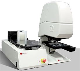
The nSPEC® is an automated, optical, inspection device geared toward defect detection and characterization of semiconductor wafers, dies and devices. It is a scanning optical microscope fully integrated with patented, image analysis processing. Never before has there been an automated machine that provides such crisp images and rich information about defects and features on semiconductor wafers. A growing number of organizations throughout the world continue to realize the value that nSPEC® provides.