EV Group (EVG), a leading supplier of wafer bonding and lithography equipment for the MEMS, nanotechnology and semiconductor markets, today unveiled a new polymer via-filling process for 3D-IC/through-silicon-via (TSV) semiconductor packaging applications.
Available on the EVG100 series of resist processing systems, the new NanoFill™ process provides void-free via filling of very deep trenches and high-aspect ratio structures, and is suitable for all common polymeric dielectrics-offering a highly flexible, low-cost and production-ready via-fill platform for interposer development for 3D-integrated image sensors and other device types.
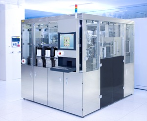 EV Group unveils a new via-filling process to improve the reliability of 3D-IC / TSV semiconductor packaging applications. Shown here is an EVG®150 automated resist processing system.
TSV interconnects are critical to the development of 3D-ICs since they enable through-chip communication between the vertically stacked device layers. Currently, most TSVs employ a solid copper via structure. However, the mismatch in coefficient thermal expansion (CTE) between the copper via and the surrounding silicon can create a high amount of stress on the via structure, which results in long-term reliability issues. Replacing copper as the conducting material is not practical due to the general ease of use of the process as well as the fact that the tooling infrastructure for copper is already well established. However, replacing the solid copper via with a partial copper-plated via that is filled with a polymeric dielectric has been demonstrated to reduce CTE mismatch and stress, thus minimizing reliability issues. EVG's proprietary process and system enable simultaneous void-free via filling and dielectric redistribution layer (RDL) formation utilizing a field-proven process technology that is compatible with all standard polymeric materials.
"3D packaging represents a fundamental change in the semiconductor industry that paves the way for continued advances in device performance and cost reduction through 'More than Moore' approaches," stated Markus Wimplinger, corporate technology development and IP director at EV Group. "EV Group has made significant investments in our portfolio of wafer-level manufacturing solutions to add new products and capabilities, such as our NanoFill solution, to help our customers accelerate the commercialization of 3D-integrated devices."
EVG's new NanoFill via-filling solution provides numerous advantages over traditional spin coating and dry lamination techniques, including providing complete via filling for permanent passivation and planarization without forming voids or cavities. The solution's ability to use all common polymeric materials provides customers with a high degree of flexibility. In addition, a sidewall passivation option is available that provides cost and throughput benefits for selected applications.
Media and analysts interested in learning more about the company and its latest developments in 3D-IC packaging and other applications at SEMICON Taiwan 2013, September 4-6, are invited to visit EVG's booth #416 in the TWTC Nangang Exhibition Hall, Taipei, Taiwan, as well as attend the company's presentations during the show's technical program. Markus Wimplinger will present "Cost-effective Thin Wafer Handling with LowTemp™ Debonding" at the SEMICON Taiwan TechXPOT on September 4 from 15:30 to 16:00, and "Trends in Wafer Bonding for High Volume Consumer MEMS Applications" at the SEMICON Taiwan MEMS Forum on September 5 from 15:10 to 15:40.
About EV Group (EVG)
EV Group (EVG) is a leading supplier of equipment and process solutions for the manufacture of semiconductors, microelectromechanical systems (MEMS), compound semiconductors, power devices and nanotechnology devices. Key products include wafer bonding, thin-wafer processing, lithography/nanoimprint lithography (NIL) and metrology equipment, as well as photoresist coaters, cleaners and inspection systems. Founded in 1980, EV Group services and supports an elaborate network of global customers and partners all over the world.
Source: http://www.evgroup.com/