The Semiconductor Metrology Systems Division (SMS) of Carl Zeiss SMT strengthens its partner- ship with the Dresden based company HAP.
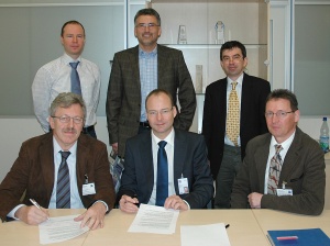 Lothar Andritzke (Managing Director HAP),
Dr. Oliver Kienzle (Managing Director Carl Zeiss SMS), Dr. Steffen Pollack (Managing Director HAP)(1st row from left to right) during the signing of the agreement supported by C. Sänn, Dr. A. Zibold,
C. Ehrlich (Carl Zeiss SMS) (2nd row from left to right).
Lothar Andritzke (Managing Director HAP),
Dr. Oliver Kienzle (Managing Director Carl Zeiss SMS), Dr. Steffen Pollack (Managing Director HAP)(1st row from left to right) during the signing of the agreement supported by C. Sänn, Dr. A. Zibold,
C. Ehrlich (Carl Zeiss SMS) (2nd row from left to right).
Both companies have signed an agreement making SMS the exclusive distributor of a recently developed “Pellicle Removal Tool” for photomasks. The system enables the automatic and gentle removal of pellicles from photomasks used in semiconductor manufacturing. Such pellicles are fundamental to protect the sensitive photomasks from contamination. The agreement marks a successful milestone in the ongoing R&D collaborations between SMS and HAP such as the development of the next generation photomask registration tool PROVE.
“We are happy to have found in HAP an innovative reliable partner, whose competencies complement ours perfectly.” states Dr. Oliver Kienzle, Managing Director of the SMS Division. “The system enables our customers to improve the cleaning process of highly sensitive photomasks, which helps to improve yields and therefore save costs”.
The company HAP develops special solutions for wafer and substrates in the microelectronic industry and micro system technique.
“The cooperation with Carl Zeiss generates strong synergies for both companies. We can participate in the worldwide sales and service network of the SMS Division as well as their comprehensive expertise in the semiconductor industry. SMS can provide its customers in the mask making industry a new technology without their own R&D effort.” explains Dr. Steffen Pollack, Managing Director HAP.
The tool automatically removes the pellicle from a photomask by applying a dedicated thermal and force recipe to the pellicle mount. This technology is highly advantageous since it eliminates the drawbacks of standard manual pellicle removal such as mask contamination, or in the worst case to the scrapping of the mask. As photomasks carry the complete structural information of integrated circuits, they are a key element in semiconductor manufacturing.