Applied Materials, Inc. today celebrates the 20th year of its Applied Endura® platform, the most successful metallization system in the history of the semiconductor industry.
Endura systems revolutionized semiconductor metallization by delivering breakthrough technologies and levels of reliability, serviceability and flexibility that far surpassed existing capabilities. The vast majority of microchips made in the last 20 years have been created using one of the over 4,500 Endura systems that have shipped across the globe to over 100 customers.
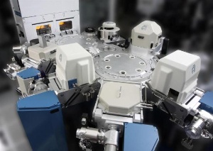 Applied Materials' Endura platform is the most successful metallization system in the history of the semiconductor industry, helping to create nearly every microchip.
“When the Endura system was first released, it set a new bar for technical performance and reliability in PVD,” said Dr. Mark Liu, senior vice president of Operations at Taiwan Semiconductor Manufacturing Company Ltd. “We rely on Endura systems and its continuous innovations in all our factories to perform a wide range of integrated PVD and CVD applications.”
Yasuo Naruke, vice president of Memory Division, Toshiba Semiconductor Company, commented, “Almost 20 years after we purchased our first Endura system, the platform continues to meet our high standards for metallization.”
The Endura system continues to set new benchmarks for the industry with the introduction today of two innovative technologies aimed at creating the leading-edge chips needed for the next generation of smart devices. The Applied Endura Avenir™ system enables chipmakers to incorporate the latest metal gate transistor technology, one of the biggest changes in transistor design since the 1970s, in their most advanced high-performance logic devices. The new Applied Endura iLB™ system advances the state-of-the-art in atomic layer deposition (ALD) to enable customers to shrink the speed-critical contact structures of 22nm and beyond logic and memory chips.
“The innovations introduced today will keep our customers at the cutting edge, enabling them to drive Moore's Law forward,” said Mike Splinter, chairman and chief executive officer of Applied Materials. “Applied’s continued investments in technology extensions and productivity upgrades have kept the Endura at the forefront of semiconductor fabrication through many chip generations. Over 85% of the Endura systems shipped to customers in the past 20 years are still in operation today – a testament to the engineers at Applied whose innovation and dedication produced a system that is such an essential part of the semiconductor industry’s past, present and future.”
Endura Innovation for Today and the Future
The new Applied Endura Avenir RF PVD1 system sequentially deposits the multiple metallic layers that form the heart of a metal gate transistor. Using proprietary radio frequency-enhanced PVD technology, the Avenir system can deposit sub-nanometer films with precisely-engineered interfaces to minimize leakage current and maximize switching speed. In addition to RF PVD, the system’s flexible, high-productivity platform can be configured with a wide range of PVD, CVD2 and ALD technologies, making it uniquely capable of fabricating all metal gate film stack structures in a single pass. The Endura Avenir system has already achieved tool-of-record status at leading logic and foundry customers for 22nm pilot production.
Minimizing the resistance of the interconnections between transistors or memory cells is essential to the fabrication of reliable, high-speed microprocessors and memory chips. A key challenge below 32nm is finding a cost-effective way to deposit a very thin barrier film layer to enable subsequent tungsten fill. The Applied Endura iLB PVD/ALD system meets this challenge using proprietary radical-enhanced ALD (RE-ALD™) technology to deposit ultra-thin, robust TiN3 films with remarkable uniformity even in very deep trenches with aspect ratios above 20:1. The system is currently the tool-of-record at major logic manufacturers and is being used for advanced DRAM development.
Source: http://www.appliedmaterials.com/