Cadence Design Systems, Inc. (NASDAQ: CDNS), a leader in global electronic design innovation, today announced that Fujitsu Limited has adopted the Cadence® Encounter® Conformal® ECO Designer to cut costs and reduce design time in its engineering change order (ECO) implementation flow.
The technology giant recently deployed the Cadence technology to tape out a network-control large-scale integration design of 40 million gates at a 65-nanometer process.
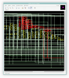 Encounter Conformal ECO Designer
“We are very pleased with our recent success using the Encounter Conformal ECO Designer,” said Takeo Asakawa, General Manager, LSI Development Div, in the Next Generation Technical Computing Unit of Fujitsu. “We had to implement several ECOs, some of them with 4,000 instances and they were very complex. I have no doubt the technology saved us significant time and resources.”
Encounter Conformal ECO Designer can play a significant role in speeding time to market and boosting design quality for companies seeking to narrow the productivity and profitability gaps outlined in the EDA360 vision. The software helps design teams implement RTL ECOs for pre- and post-mask layout. It combines automatic ECO analysis and design netlist modification with world-class equivalence checking to boost performance and productivity. This unique technology combines logic equivalence checking with functional ECO analysis and generation, design netlist modification, clock domain synchronization, and semantics checks.
By using Encounter Conformal ECO Designer Fujitsu was able to start implementation before functional verification was completed, cutting total development time by months. Even engineers not familiar with logic design can tackle ECOs to implement late-stage changes needed to improve design quality prior to manufacturing.
“Fujitsu’s recent success with the Encounter Conformal ECO Designer is a good example of the time-to-market and quality benefits that the right technology can bring to the path toward Silicon Realization,” said Bassilios Petrakis, director of product management at Cadence. “Like many of our other customers, Fujitsu was able to exploit this technology to give itself a competitive boost.”
Source: http://www.cadence.com/