Posted in | News | Nanoelectronics

Endura Avenir Platform Increases 22nm Transistor Contacts

Applied Materials has recently added to the applications of its Applied Endura Avenir RF PVD platform to incorporate  deposition of nickel-platinum (NiPt) alloys, to increase transistor contacts scaling to the 22nm technology node.

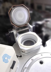
AM's Endura Avenir RF PVD platform

NiPt films enhance performance but it leaves a residue at the bottom of the high aspect ratio (HAR). The Avenir delivers consistent contact tolerance and maximum output. It delivers more than 50% bottom coverage in deep, HAR contact holes in a cost- efficient manner.

Prabu Raja, vice president and general manager of the Metal Deposition Products division, the technology offers chipmakers a safe way to develop tough, low-resistance transistor contacts for rapid construction. It will benefit contact applications in various logic and foundry scenarios.

It has been embedded into the Endura, a PVD technology with increased radio frequency that was introduced in 2010, to combine metal gate transistor technology with high-performance logic solutions. This feature allows developers to deposit consistent NiPt sheets at the lower end of slim, deep contact holes with a diameter of less than 30nm. This feature is ideal for low contact tolerance and maximum transistor performance.

Source: http://www.appliedmaterials.com

Citations

Please use one of the following formats to cite this article in your essay, paper or report:

  • APA

    Applied Materials Inc.. (2019, February 12). Endura Avenir Platform Increases 22nm Transistor Contacts. AZoNano. Retrieved on April 18, 2024 from https://www.azonano.com/news.aspx?newsID=21975.

  • MLA

    Applied Materials Inc.. "Endura Avenir Platform Increases 22nm Transistor Contacts". AZoNano. 18 April 2024. <https://www.azonano.com/news.aspx?newsID=21975>.

  • Chicago

    Applied Materials Inc.. "Endura Avenir Platform Increases 22nm Transistor Contacts". AZoNano. https://www.azonano.com/news.aspx?newsID=21975. (accessed April 18, 2024).

  • Harvard

    Applied Materials Inc.. 2019. Endura Avenir Platform Increases 22nm Transistor Contacts. AZoNano, viewed 18 April 2024, https://www.azonano.com/news.aspx?newsID=21975.

Tell Us What You Think

Do you have a review, update or anything you would like to add to this news story?

Leave your feedback
Your comment type
Submit

While we only use edited and approved content for Azthena answers, it may on occasions provide incorrect responses. Please confirm any data provided with the related suppliers or authors. We do not provide medical advice, if you search for medical information you must always consult a medical professional before acting on any information provided.

Your questions, but not your email details will be shared with OpenAI and retained for 30 days in accordance with their privacy principles.

Please do not ask questions that use sensitive or confidential information.

Read the full Terms & Conditions.