A supplier of scientific solutions and instruments for molecular and materials research, Bruker has introduced the Dimension Edge PSS atomic force microscope (AFM) for patterned sapphire substrate (PSS) measurement in order to manufacture high-brightness light-emitting diode (HB-LED).
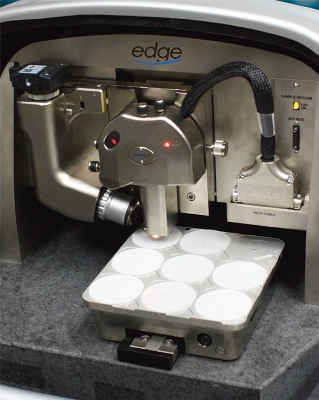 Dimension Edge PSS with AutoMET software and 9 wafer chuck
The Dimension Edge PSS is a production-environment, an easy-to-use AFM specifically designed for delivering resolutions better than conventional optical techniques as well as offering accurate three-dimensional profile data to handle sophisticated PSS processes. The system carries out automated report generation, data analysis, information collection and measurement on 2 to 6” wafers for applications in production metrology. Also, it improves AFM features required for LED R&D.
The system is available in combination with Bruker’s AutoMET software package designed particularly to meet the manufacturing requirements of HB-LED producers. It is possible to configure the software to enable measurement of one to nine wafers at several points of each wafer. It also largely improves manufacturing yield by enabling automated data analysis and report generation, offering measurement data to the engineer and a fail/pass indicator to the technician operator.
Mark R. Munch, Bruker Nano Surfaces Division’s President stated that manufacturers of HB-LED are seeking PSS technology to improve critical production processes and the Dimension Edge PSS AFM is helpful in monitoring those enhanced processes. The system’s unmatched resolution, precision and measurement speed offers quick process feedback, he added.
David V. Rossi, VP and GM of Bruker’s AFM Business, stated that with the launch of the Dimension Edge PSS, the company continues to illustrate its dedication to improve AFM performance and application for both manufacturing and researcher environments.
Source: http://www.bruker-axs.com/