The Lawrence Berkeley National Laboratory has developed the Semiconductor High-NA Actinic Reticle Review Project (SHARP) microscope for photolithography. The SHARP microscope is an advanced extreme-ultraviolet (EUV) photomask-imaging microscope which has been developed in partnership with semiconductor manufacturers.
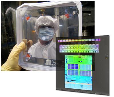 Kenneth Goldberg is seen in the reflective coating of a photolithography mask which he's about to measure at the Advanced Light Source's beamline 11.3.2. Inset at lower right shows a mask's extreme-ultraviolet (EUV) absorbing layer, printed on a six-inch square of glass coated with multiple layers of molybdenum and silicon only billionths of a meter thick to reflect unwanted EUV. The patterned layer represents one level of a working microprocessor or memory chip, which may have 20 or more such levels. Its structures are less than one ten-millionth of a meter across and diffract visible light in rainbow patterns. Credit: Lawrence Berkeley National Laboratory
Kenneth Goldberg at the Berkeley Lab's Materials Science Division Center for X-Ray Optics (CXRO) is leading the 1.5-year, $4.1 million project. The EUV microscope is to be used simultaneously along with the Advanced Light Source microscope at beamline 11.3.2. The Actinic Inspection Tool (AIT) microscope has specific imaging capabilities, but may not be able to meet future requirements. SHARP would be better than the AIT in terms of speed, resolution, coherence control and illumination.
Semiconductor devices of the near future will measure in terms of billionths of a meter for example, 8, 11 or 16 nm. Mass production of such semiconductors requires a 13.5 nm wavelength EUV light for photolithography. Photomasks play a major role in mass production in lithography. Master circuit patterns are carried by a series of photomasks and are transferred layer by layer onto chips for creation of semiconductor devices.
Dust particles or imperfections on the master circuit patterns can lead to chip failure. EUV microscopy can reliably identify such particles and defects when compared to non-EUV inspection tools. It can help evaluate defects and repair mask architectures and materials, advanced pattern features and strategies.
The SHARP EUV microscope has high-magnification objective lenses, which are holographic Fresnel zoneplate lenses. CXRO's Nanowriter produces these lenses, which have a width, slightly more than a single human hair. These microscopic lenses can project images with a 2,000x magnification. Illumination coherence control is a unique feature of the microscope. The EUV beam produced has a laser-like coherence. Re-engineering the illumination into a partial coherence state can improve the image resolution for microscopy. The beamline illuminator in the SHARP microscope has an angle-scanning mirror that can maneuver the highly-coherent ALS light into patterns and break and re-shape the coherence properties.
Source: http://www.lbl.gov/