Scientists at the Lawrence Berkeley National Laboratory (Berkeley Lab) of the U.S. Department of Energy have devised a potential low-cost method for synthesizing stretchable and flexible backplanes at a large-scale utilizing semiconductor-enhanced carbon nanotube solutions, which provide thin-film transistor networks with superior electrical properties and higher charge carrier mobility when compared to that of organic-based devices, paving the way to develop future plastic electronic devices.
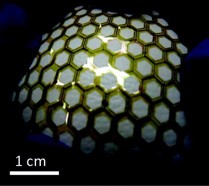 This optical image of flexible and stretchable thin film transistor array covering a baseball shows the mechanical robustness of this backplane material for future plastic electronic devices. (Image courtesy of Berkeley Lab)
Ali Javey, who serves as a professor of computer science and electrical engineering at the University of California Berkeley as well as a faculty scientist at the Materials Sciences Division of Berkeley Lab, stated that by using their solution-based processing technology, the researchers have fabricated mechanically stretchable and flexible active-matrix backplanes on the basis of highly uniform and completely passivated sequence of thin-film transistors made of single- walled carbon nanotubes. This technology along with inkjet printing of metal contacts is capable of offering lithography-free production of inexpensive stretchable and flexible electronics in the coming years, he said.
In order to fabricate their active-matrix backplanes, the researchers utilized a single-walled carbon nanotube solution containing 99% of semiconductor single walled carbon nanotubes, which provides a superior on/off ratio of roughly 100 for the backplanes. The researchers used laser to form hexagonal holes in honeycomb patterns in a thin flexible substrate made of polymide so that it now becomes stretchable. They then completed the fabrication of their backplanes by depositing semiconductor-enhanced single walled carbon nanotubes subsequent to the deposition of aluminum and silicon oxide layers over the substrates.
Toshitake Takahashi, one of the researchers, stated that in the future, the magnitude of directionality and stretchability of the substrate can be adjusted by either optimizing the design of the mesh or modifying the size of the hole.
The scientists have built an artificial electronic skin (e-skin) that can sense and respond to touch for exhibiting the efficacy of their carbon nanotube backplanes. The e-skin for spatial pressure mapping comprises a sequence of 96 sensor pixels having an area of 24 sq. cm, with every pixel being dynamically manipulated by an individual thin film transistor. The researchers then placed an L-form weight over the e-skin sensor array with a standard pressure of roughly 15 kPa for pressure mapping.
Takahashi stated that the new e-skin sensor array demonstrated a three-fold increase in sensitivity in the linear operation regime when compared the earlier e-skin sensors developed by the researchers. This enhanced sensitivity was due to the enhanced device performance caused by the single walled carbon nanotube backplanes, he said. In the coming years, this backplane technology can be expanded by integrating several sensors and other devices for the development of multipurpose artificial skins. This technology can also be utilized for flexible displays, he said.
Source: http://www.lbl.gov