STMicroelectronics has declared that it has successfully produced first-of-its-kind semiconductor wafer, whose dice were completely tested devoid of contact probes.
 STMicroelectronics Produces World's First Semiconductor Wafer Using EMWS Technology
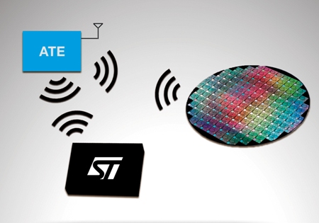
STMicroelectronics’ sophisticated testing technology allows the testing of a wafer-based chip such as RFID ICs utilizing electromagnetic waves as the only connection to the circuit arrays on the wafer, offering several benefits, including lower product cost, shorter testing times and higher yields. Moreover, this contactless method enables the testing of RF circuits under conditions comparable to conditions of real applications.
The novel electromagnetic wafer sort (EMWS) technology is an outcome of UHF TAG Antenna Magnetically Coupled to Integrated Circuit (UTAMCIC), a joint research and development project of STMicroelectronics and the University of Catania.
The EMWS technology is an advancement of electrical wafer sorting, wafer production’s final stage prior to assembling and testing of the finished packaged products. At this production cycle stage, the processed wafer comprises an identical circuit array dubbed die. The tiny probes of a probe card linked to Automatic Test Equipment (ATE) are made to touch the test pads over the die by moving the card over every die. The ATE then tests each die for its functionality, which allows the rejection of non-functional die prior to its assembling and packaging.
In the EMWS technology, individual dice comprise a microscopic antenna and the ATE provides power and corresponds through electromagnetic waves with the dice. This method decreases the count of test pads over the die, resulting in the reduction of die size. This technology is capable of performing completely contactless testing of low-power circuits, which in turn eliminates the damage of test pads and improves the yield. Moreover, the test cycle time can be reduced significantly thanks to the ability to achieve high testing parallelism in the contactless mode.
Source: http://www.st.com