A microscopic study led by An-Ping Li from the Oak Ridge National Laboratory of the Department of Energy has demonstrated that single atoms can turn on or off electronic properties of quantum nanowires, one of the tiniest recognized conductors in the world.
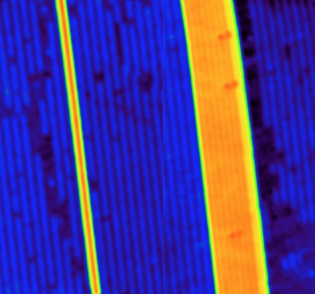 A one-dimensional quantum nanowire (seen in yellow on left) can turn from a conductor to an insulator with the addition of a single atomic defect, according to microscopic analysis from Oak Ridge National Laboratory. Bundles of nanowires (right) are generally more stable, leading to better conductance. (credit: An-Ping Li and Shengyong Qin/ORNL)
The research team has explained the impact of the conducting nanowires’ atomic structure on their electronic behavior using multiple-probe scanning tunneling microscopy. It showed that a conducting nanowire can be converted into an insulator by closing the electron path through the intentional introduction of defects of a single atom size. It studied nanowires made of gadolinium silicide (GdSi2).
According to Li, GdSi2 nanowires are one-dimensional conductors that can be used as a basic component in quantum electronic architectures. Their compatibility with traditional silicon technology facilitates their use in nanoelectronic devices. A conductor becomes highly sensitive to atomic defects when it is very small. Electrons are able to find an alternative path if the wire or conductor is large. However, electrons have no path to escape with a tiny nanowire. When a few defects are introduced into this nanowire, they turn off the conductance of the nanomaterial, thus making it an insulator, Li explained.
The research team discovered a different behavior in nanowire bundles comprising two or more nanowires, which are isolated at only a few angstrom distances. Li explained that the interwire coupling of the nanowire bundles delivers a stabilizing effect to the structure, thus making it a better conductor. It is the first correlated analysis that relates electron transfer to structural components such as single point impurities or defects that are deliberately developed in the nanowires.
The study findings have been reported in Nano Letters, a journal of the American Chemical Society.
Source: http://www.ornl.gov