May 3 2012
Strong metals have a tendency to be less ductile - unless the metal happens to be a peculiar form of copper known as nanotwinned copper. The crystal structure of nanotwinned copper exhibits many closely-spaced interruptions in an otherwise regular atomic array. These interruptions, despite being termed 'defects', actually increase the metal's strength without reducing its ductility, making it attractive for applications such as semiconductor devices and thin film coatings. However, the relationship between the properties of these defects and those of the metals containing defects remains unclear.
Now, Zhaoxuan Wu and co-workers at the A*STAR Institute for High Performance Computing have now performed a large-scale numerical simulation that sheds light on this relationship. The simulation addressed some of their previous, unexplained experimental data.
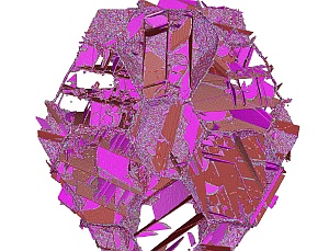
 The image shows the simulation of a polycrystalline nanotwinned copper and its defects during tensile loading. Image courtesy of Elsevier.
In 2009, the researchers had observed that the strength of nanotwinned copper reached a maximum when the size of the defects in its crystal structure was about 15 nanometers. When the defects were made smaller or larger, the copper's strength decreased. This contradicted the classical model, which predicted that the metal's strength would increase continually as the defect size was reduced.
Wu and co-workers addressed this contradiction by using a very large-scale molecular dynamics simulation to calculate how a nanotwinned copper crystal consisting of more than 60 million atoms deforms under pressure. They observed that its deformation was facilitated by three types of mobile dislocations in its crystal structure. Significantly, they found that one of these three types of dislocation, called a 60° dislocation, interacted with defects in a way that depended on the defect size.
The 60° dislocations were able to pass through small defects in a continuous manner, creating many new, highly mobile dislocations that softened the copper. On the other hand, when they encountered large defects, a three-dimensional dislocation network formed that acted as a barrier for subsequent dislocation motion, thus strengthening the copper. The simulation predicted that the critical defect size separating these two regimes of behavior occurred at 13 nanometers, very close to the experimentally measured value of 15 nanometers.
The results show that there are many different deformation mechanisms occurring in nano-structured materials like nanotwinned copper. Understanding each of them will allow scientists to tune material properties - as Wu comments: "For example, we could introduce dislocation barriers to stop their motion, or change defect interface energies to change how they deform." Wu adds that the next step for his research team will be to take into account the diversity in defect sizes within a single material.
Source: a-star.edu.sg