Massachusetts Institute of Technology (MIT) researchers have reported that they have discovered methods of developing defect-free patterns of nanocrystal films. They have controlled the position and shape of the nanocrystal films with nanoscale resolution.
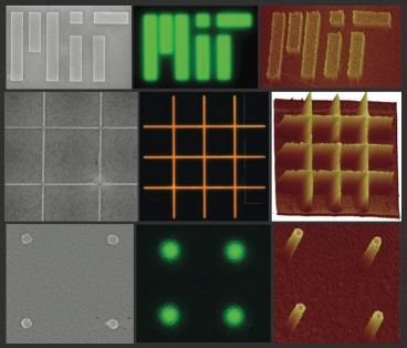 Images of nanopatterned films of nano crystalline material produced by the MIT research team. Each row shows a different pattern produced on films of either cadmium selenide (top and bottom) or a combination of zinc cadmium selenide and zinc cadmium sulfur (middle row). The three images in each row are made using different kinds of microscopes: left to right, scanning electron microscope, optical (showing real-color fluorescence), and atomic force microscope. Images courtesy of Mentzel et al, from Nano Letters
Semiconductor nanocrystal films hold promise for a range of applications including high-resolution display screens, biomolecule detectors, solar cells and photonic and electronic circuits. Producing structurally uniform films is not easy as it is difficult to control nanocrystal placement on surfaces. Further, cracks occur in conventional nanocrystal films.
The researchers tried to understand the movement of electrons in nanocrystal arrays, as control over array formation has been limited. Precise control over nanocrystal production allows production of materials that fluoresce in various colors due to difference in sizes.
Initially, nanoscale patterns that emitted light in the invisible infrared range were produced. Later, semiconductor nanocrystal patterns were made to glow, which was visible through optical microscopes. The defect-free films had electrical conductivity that was over 180 times that of conventional cracked films. These tiny patterns of defect-free films were achieved by leaving a thin polymer layer on a silicon dioxide substrate and nanocrystal layer was deposited over it.
The nanocrystal patterns allow the nanocrystals to be used for broad-spectrum solar cells due to their ability to absorb light colors across a wide spectrum. The researchers plan to study elementary processes of solids using the arrays. Further, these materials can be used for developing sensitive detectors for biological molecules in medical screening systems.
Source: http://web.mit.edu/