Jan 8 2018
It is most important to ensure that carbon nanotubes used for electronics are extremely clean to increase their application in futuristic nanoscale devices. Researchers from Rice and Swansea universities have discovered a method to eliminate contaminants from the nanotubes.
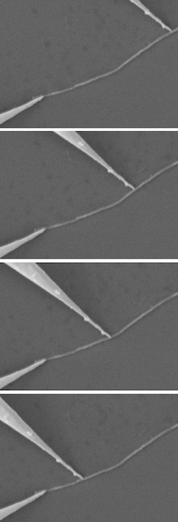 Scientists at Rice and Swansea universities used tungsten probes attached to a scanning tunneling microscope to test the conductivity of carbon nanotubes before and after treatment to decontaminate them. The sequence above shows one probe at the end and the other moving along the length of an isolated nanotube. (Photo credit: Courtesy of the Barron Research Group)
Andrew Barron, a Rice chemist and also a professor at Swansea University in the United Kingdom, and his colleagues have found out the way to make nanotubes clean. In the meantime, they also found out the reason behind the difficulty in evaluating electrical characteristics of nanotubes.
Similar to a normal wire, semiconducting nanotubes are progressively more resistant to electric current across their length. However, for many years, evaluations of conductivity of nanotubes have not been consistent. The Rice-Swansea researchers strived to find the reason behind this.
“We are interested in the creation of nanotube-based conductors, and while people have been able to make wires, their conduction has not met expectations,” stated Barron. “We wanted to determine the basic science behind the variability observed by other researchers.”
The team found out that hard-to-eliminate contaminants such as carbon, leftover iron catalyst, and water can easily impact the outcomes of conductivity tests. According to Barron, removing those contaminants opens the door for innovative applications of carbon nanotubes in nanoscale electronics.
The new research has been reported in the Nano Letters journal published by the American Chemical Society.
The team initially developed multiwalled carbon nanotubes with a diameter of 40-200 nm and a length of up to 30 mm. Then, the nanotubes were either heated in vacuum or bombarded by using argon ions to make their surfaces clean.
The team investigated each nanotube similar to the way any electrical conductor is investigated: they touched them with two probes to observe the amount of current that travels through the material from one tip to the other. In this study, tungsten probes were affixed to a scanning tunneling microscope.
In the case of clean nanotubes, resistance progressively increased with increase in the distance, as is usually the case. However, the outcomes were altered when the probes got in touch with surface contaminants, thereby increasing the electric field strength at the tip. Moreover, when measurements were conducted within 4 mm of one another, regions with decreased conductivity formed due to the contaminants overlapped on one another, thus altering the outcomes more.
“We think this is why there’s such inconsistency in the literature,” stated Barron. “If nanotubes are to be the next-generation lightweight conductor, then consistent results, batch-to-batch and sample-to-sample, are needed for devices such as motors and generators as well as power systems.”
Heating the nanotubes to more than 200 °C, or 392 °F, in vacuum decreased the surface contamination. However, it was not adequate to prevent inconsistent outcomes, discovered the team. Although bombarding with argon ion made the tubes clean, it resulted in an increase in flaws that decrease the conductivity.
Eventually, the team found out that when the nanotubes were vacuum annealed at 500 °C, or 932 °F, the contaminants were adequately reduced to precisely evaluate the resistance.
According to Barron, engineers using nanotube films or fibers in devices at present change the material by doping or other methods to achieve the needed conductive characteristics. However, upon adequate decontamination of the source nanotubes, they must be in a position to achieve the desired conductivity by just placing their contacts in the correct position.
“A key result of our work is that if contacts on a nanotube are less than 1 micron apart, the electronic properties of the nanotube change from conductor to semiconductor, due to the presence of overlapping depletion zones, which shrink but are still present even in clean nanotubes,” stated Barron.
“This has a potential limiting factor on the size of nanotube-based electronic devices,” he stated. “Carbon-nanotube devices would be limited in how small they could become, so Moore’s Law would only apply to a point.”
The lead author of the study is Chris Barnett from Swansea University. Cathren Gowenlock and Kathryn Welsby, and Rice alumnus Alvin Orbaek White from Swansea are the co-authors of the study. Barron is the Charles W. Duncan Jr.–Welch Professor of Chemistry and a professor of materials science and nanoengineering at Rice and the Sêr Cymru Chair of Low Carbon Energy and Environment at Swansea.
The study was supported by the Welsh Government Sêr Cymru National Research Network in Advanced Engineering and Materials, the Sêr Cymru Chair Program, the Office of Naval Research, and the Robert A. Welch Foundation.