Jan 29 2018
In order to observe the driving force behind the unusual behavior in atomically thin materials and discover the result of stacking them in various combinations with different ultrathin materials, researchers have to monitor their characteristics at the smallest possible scales.
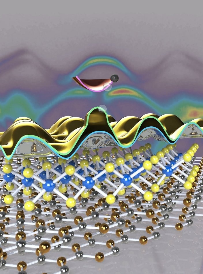 This rendering shows a “ball-and-stick” representation of the atomic structure of a 2-D single crystalline layer of tungsten disulfide (blue and yellow), on top of layers of 2-D boron nitride (silver and gold). On top of these is a representation of the structure of electronic energy levels (valence bands) within the tungsten disulfide and the increased splitting between the two valence bands observed using an x-ray technique at the MAESTRO beamline. The experiments suggest the effect could be due to “trions,” made up of two holes and an electron in the bands - depicted as clear and dark spheres. The background is raw data of the electronic structure of the tungsten disulfide, as measured in the experiment. (Image credit: Chris Jozwiak/Berkeley Lab)
Access Microscopic and Electronic Structure Observatory (MAESTRO) - a next-generation X-ray experiment platform at the Advanced Light Source (ALS) at the Department of Energy’s Lawrence Berkeley National Laboratory (Berkeley Lab) - offers innovative microscale observations of this peculiar 2D realm.
Scientists have now set their sight on signatures of the striking behavior of electrons in a 2D material at microscale resolution and have reported this in the Nature Physics journal January 22, 2018.
The new knowledge acquired from these experiments indicate that the characteristics of the analyzed 2D semiconductor material, known as tungsten disulfide (WS2), might be largely adjusted, with prospective applications in electronics and various forms of information storage, processing and transfer.
These applications can include next-generation devices developed from emerging research fields such as excitonics, spintronics and valleytronics. In such fields, scientists attempt to exploit characteristics (such as momentum and energy levels) of electrons and counterpart particles in a material, for effective transfer and storage of information - similar to the flipping of 1s and 0s in traditional computer memory.
For instance, spintronics is dependent on the manipulation of an intrinsic characteristic of electrons and not their charge. Excitonics can multiply charge carriers in devices to enhance the efficiency of LED lighting and solar panels. Valleytronics could use separations in the electronic structures of a material as unique pockets or “valleys” for storage of information.
The signal measured by using MAESTRO indicated a considerably increased splitting between two “bands,” or energy levels, related to the electronic structure of the material. Such an increased splitting finds prospective use in spintronics devices.
WS2 has hitherto been known to strongly interact with light as well. The innovative outcomes, together with its earlier known characteristics, render it a propitious material for application in optoelectronics, where electronics can be adopted to regulate the release of light and vice versa.
These properties could be very exciting technologically... (The latest research) in principle shows the ability to change these key properties with applied electric fields in a device.
The ability to engineer the features of the electronic structures of this and other materials could be very useful in making some of these possibilities come true. We are right now at the brink of being able to study a huge variety of materials, and to measure their electronic behavior and study how these effects develop at even smaller scales.
Chris Jozwiak, Co-Lead Author
The research also indicates that trions - striking three-particle combinations of electrons and excitons (which are bound pairs of electrons) and “holes,” their oppositely charged counterpart - could throw light on the effects they evaluated in the 2D material. Electrons as well as holes function as charge carriers in semiconductors seen in popular electronic devices.
Scientists adopted a form of angle-resolved photoemission spectroscopy (ARPES) at the MAESTRO beamline to remove electrons from samples by using X-rays and gain an understanding of the electronic structure of the samples by knowing the energy and direction of the ejected electrons. The method can throw light on the way electrons in the material interact with one another.
“There are very few direct observations of a particle interacting with two or more other particles,” stated Eli Rotenberg, a senior staff researcher at ALS who conceptualized MAESTRO over 10 years ago. It was constructed with the aim of direct and detailed viewing of such “many-body” interactions not feasible earlier, he stated. “This is what we were going for when we built the MAESTRO beamline.”
MAESTRO, which was made accessible to researchers in the year 2016, also presents various stations that enable the researchers to create and control samples for X-ray investigations while preserving sterile conditions that prevent contamination. MAESTRO is one of many X-ray beamlines at the ALS specialized for samples such as vaccines, proteins, meteorites, and batteries.
According to Jozwiak, apart from MAESTRO’s accurate evaluations, the cautious preparation of the tungsten disulfide flakes in sizes adequate for the analysis and their shift to a base material or substrate does not hinder their electronic characteristics or impede the X-ray evaluations that were also important in the success of the recent research.
Two-dimensional materials are extremely sensitive to their surroundings, so it’s imperative to fully understand the role of any outside disturbances that affect their properties.
Jyoti Katoch, Lead Author
Katoch collaborated with Roland Kawakami, a physics professor at Ohio State, in formulating the samples and designing the experiment. They combined WS2 samples with boron nitride, which gave rise to a non-interacting, stable platform that was very important for the X-ray evaluations. Subsequently, they used a metal as an “external knob” to alter the characteristics of WS2.
“This study enables two critical breakthroughs: it provides a clear fundamental understanding of how to remove outside effects when measuring the intrinsic properties of 2-D materials, and it allows us to tune the properties of 2-D materials by simply modifying their environment.”
Søren Ulstrup, an assistant professor from Aarhus University who was part of the WS2 MAESTRO experiments as a postdoctoral researcher, stated, “Seeing the intrinsic electronic properties of the WS2 samples was an important step, but perhaps the biggest surprise of this study emerged when we started to increase the number of electrons in the system—a process called doping.”
“This lead to the dramatic change of the splitting in the band structure of WS2,” he added, which indicates the presence of trions.
According to Rotenberg, MAESTRO has the ability to deal with samples of very small sizes in the order of tens of microns, which is also important in analyzing this and other 2D materials. “There’s a big push to resolve materials’ properties on smaller and smaller scales,” he stated, to have an in-depth knowledge of the basic characteristics of 2D materials. Moreover, at present, researchers are striving to push MAESTRO’s potentials to analyze even smaller features, at the nanoscale level.
Jozwiak stated R&D for stacking 2D layers to customize their characteristics for specialized applications has gained momentum and MAESTRO is most appropriate for evaluating the electronic characteristics of these stacked materials, too.
We can see a very explicit impact on properties by combining two materials, and we can see how these effects change when we change which materials we’re combining.
There is an endless array of possibilities in this world of ‘2-D Legos,’ and now we have another window into these fascinating behaviors.
Chris Jozwiak, Co-Lead Author
The Advanced Light Source is a DOE Office of Science User Facility.
Scientists from the U.S. Naval Research Laboratory, Ohio State University, and Aarhus University in Denmark also contributed to the study. Samples used in the research were developed at the U.S. Naval Research Laboratory and processed for experiments at Ohio State University.
The U.S. Department of Energy’s Office of Basic Energy Sciences, the Danish Council for Independent Research, VILLUM FONDEN, the Swiss National Science Foundation, the National Science Foundation, the U.S. Naval Research Laboratory Nanoscience Institute, and the U.S. Air Force Office of Scientific Research supported the study.