Applied Materials, Inc. today announced its Baccini Esatto Technology™, a high precision, multi-step screen printing capability for Applied's market-leading Baccini back-end solar cell processing systems. Featuring proprietary hardware and software innovations, the Esatto Technology is designed to increase the efficiency of crystalline silicon (c-Si) solar cells by enabling the fabrication of advanced contact structures. The first of several applications of the Esatto Technology is for double-printed metal line deposition where it has been shown to raise absolute cell efficiency by as much as 0.5%.
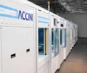
 The Baccini Esatto Technology enables the fabrication of advanced contact structures to increase the efficiency of crystalline silicon solar cells. (Photo: Business Wire)
“Currently being used in customer production, Esatto Technology demonstrates our commitment to rapidly advance crystalline silicon technology by providing comprehensive solutions that enable higher efficiency,” said Davide Spotti, vice president and general manager of Applied's Baccini Cell Systems division. “Working with leading suppliers to optimize consumable materials and printing techniques, we've created a unique capability to help customers quickly deploy advanced cell patterns in production environments and bring their higher value products to market.”
The Baccini Esatto Technology provides customers with a cost-effective upgrade to their current and future Baccini back-end systems with proven reliability and high repeatability. The result of several proprietary hardware and software innovations including high resolution imaging, screen alignment, and advanced process control, the Esatto Technology allows multiple layers of different materials to be overlaid with better than ±15µm repeatability.
Esatto Technology was designed to enable advanced contact formation techniques such as double-printed frontside metal lines and the multiple process flows required to create selective emitter structures. The first application of Esatto Technology in production is for double-printed metal lines. This application enables manufacturers to print taller, narrower grid lines, thus reducing the shadowing effect caused by wide grid lines while improving electrical conductivity. In a production environment, Esatto Technology allowed the replacement of single 120µm wide lines with two-layer, double-height lines less than 80µm wide on the finished cell.
For more information on the full line of Applied Baccini solutions for crystalline silicon solar cell manufacturing, visit www.appliedmaterials.com/products/solar_crystal_silicon_3.html.
Applied Materials, Inc. (Nasdaq:AMAT) is the global leader in Nanomanufacturing Technology™ solutions with a broad portfolio of innovative equipment, service and software products for the fabrication of semiconductor chips, flat panel displays, solar photovoltaic cells, flexible electronics and energy efficient glass. At Applied Materials, we apply Nanomanufacturing Technology to improve the way people live.