Applied Materials, Inc., the global leader in Nanomanufacturing Technology™ solutions with a broad portfolio of innovative equipment, service and software products for the fabrication of semiconductor chips, flat panel displays, solar photovoltaic cells, flexible electronics and energy efficient glass, today unveiled its Applied iSYS™ platform, the industry's first fully-integrated abatement and vacuum pumping solution for controlling emissions in the semiconductor fab.
Networked with an Applied process tool, the iSYS system can deliver typical annual savings in power, water and gas consumption equivalent to 200MWh of energy or 220,000 pounds of CO2 emissions, compared to currently available configurations. In addition to having environmental benefits, the iSYS system lowers the utility cost for abatement and vacuum pumping on a process tool by more than 20%.
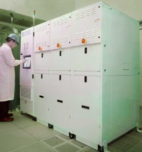
 The Applied iSYS platform is the industry's first fully-integrated abatement and vacuum pumping solution for controlling emissions in the semiconductor fab. (Photo: Business Wire)
Key to the iSYS platform's capability to conserve resources is its unique control system that is synchronized with the wafer processing tool, sensing real-time changes in each process chamber and directing subsystems into pre-defined standby states. Utility metering sensors and software are built into every iSYS platform to enable remote monitoring of cumulative energy savings and to track progress in reaching energy sustainability targets.
“With the iSYS platform Applied is capitalizing on its unmatched equipment automation and process tool technology to create a smart solution for decreasing waste in semiconductor manufacturing,” said Charlie Pappis, vice president and general manager of Applied Global Services. “By modulating resource consumption in response to changing tool conditions, the iSYS platform can help our customers lower their operating costs and support sustainable manufacturing practices.”
The highly-compact Applied iSYS unit can be installed in less than one day and consumes 40% less floor space than non-integrated systems. Designed from the outset for maximum ease of servicing, the iSYS design consolidates major components and eliminates redundancy to greatly reduce the number of external connections while optimizing maintenance ergonomics. By stacking lighter components above heavier ones and optimizing duct routing, technicians can quickly complete all service tasks, including pump replacement, without special equipment.
The substantial energy saving achieved by the iSYS platform was measured at Applied's advanced Maydan Technology Center on an Applied Producer® GT™ PECVD* system using SEMI S23 methodology. Initially launched for Applied Materials' CVD systems, the flexible iSYS architecture can also support etch applications.
* PECVD = plasma enhanced CVD