The integration of semiconductor design and fabrication with photonics is enabling the advancement of both fields in new, exciting directions. This new hybrid field, silicon photonics, also known as SiP, is one more step in years of extensive product developments, where photonic interconnects have gradually improved, resulting in the following changes in communications technologies:
- Copper trunks were replaced by transcontinental fibers, reducing costs and allowing digital data communications
- Satellite communications links were replaced by transoceanic fibers, offering more capacity with lower latency
- Regional photonic networks introduced bandwidth and allowed interconnectivity in developed countries
- Fiber to the home brought broadband to neighborhoods, and regional photonic networks allowed dense connectivity for cities and industry
Today, the increasing need for energy, as well as increasing bandwidth usage thanks to cloud services, has pushed the trend even further, resulting in the emergence of photonic interconnects for data centers.
The latest silicon design and fabrication technologies, which integrate both electronic and photonic devices on a chip, render an additional benefit in terms of efficiency, bandwidth, and functionality.
These devices also present a number of challenges during device testing. During electrical testing of standard microcircuits, un-diced chips are physically contacted on the fully-patterned wafer by means of electrode probe arrays.
It is often sufficient to position the probes for these chips to micron scale precisions, and hence traditional positioning control and vision technologies are adequate for carrying out both testing and probing at sufficient speeds so as make the entire process viable economically.
In contrast, testing of photonic devices needs nanoscale and non-contact alignment between a probe fiber and the device being tested.
In the interim, multiple devices may be involved in final packaging alignments, each needing nanoscale alignment to each other, usually in multiple degrees of freedom. Present-day devices such as waveguide elements include multiple outputs and inputs, where some or all have to be aligned and kept in a repeatable and consistent configuration for work to be carried out.
In addition, in spite of the increasing challenges and growing resolution needs of photonic probing, testing and packaging, throughputs have to be extremely high for the economic goals of the manufacturing process to be fulfilled.
Fast Multi-channel Photonics Alignment Engine / Silicon Photonics Test Platform www.pi.ws
Video demonstration of an in-wafer, grating-coupled waveguide device is simulated by a short length of single-mode fiber. Its input and output are coupled via lensed fibers mounted on grippers on PI’s Nanocube XYZ piezo positioner / scanner, which is controlled by the E-712 controller.
The Background
Photonic alignment processes are divided into two categories:
- Quick areal scans of a single device against another (probe fiber) to construct an overall shape of the coupling (Figure 1)
- The gradient search from which the path to optimum is interpreted. This gradient search inflicts a tiny patterned motion of a single device against the other
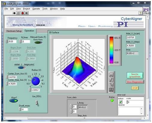
Figure 1. Full-field areal scan
The goal of both these processes is to localize the mutual direction at which combined optical throughput is improved, and both can thus be applied to angular, longitudinal (Z) and transverse (XY) optimizations.
The benefit of gradient searches is that they make it possible to track and prevent drift and rectify disturbances; however, they need a clean coupling or else they may lock onto a local maximum.
The implementation of rapid scans proves helpful in ascertaining the estimated location of a coupling’s main mode. This not only promotes a hybrid approach where the gradient search is initiated within the area of the global maximum, but also aids in preventing the local maxima completely.
In photonics testing and packaging applications, removal of drift and continuous optimization are usually preferred. Therefore, the gradient search plays a key role in majority of implementations.
Traditional analog implementations of the gradient search were followed in laboratory-class applications where their low cost and excellent speed and flexibility proved to be a perfect match. However, in case of production-class applications, a digital implementation is favored because these are limitable, with each motion being the outcome of a calculation.
Patented in the early 1990s, the first digital gradient search has been at the forefront of photonics packaging automation, but it can only be used in sequence to the couplings in an optical train.
This sequential approach increases the time needed to line up a device by some multiple of the number of outputs and inputs, with the multiplier based on the degrees of freedom involved in every coupling optimization. This presented an impractical option for producing present-generation of complex SiP devices.
The Breakthrough
Thanks to the introduction of an on-the-fly version of the digital gradient search in the late 2000s, the patented CyberTrack from PI can carry out complete limitable and metrical alignment processes by means of continuous motion patterns. In addition, the alignment method can even be used with the asymmetrical and astigmatic coupling profiles, which are common in emerging devices.
This makes it possible to carry concurrent alignments as well as tracking optimization of different outputs and inputs in photonic devices, with each device in manifold degrees of freedom. The capability to align M outputs and N inputs in P degrees of freedom is almost independent of M, N and P, yet the process continues to remain limitable and metrical.
The latest NxM alignment optimization technology is not only easy to use and implement, but also delivers fab-worthy alignment repeatability, performance, and speed. The technology is completely automatic and transparent, and is an established technology for production test and packaging automation of SiP devices.
It is internalized in PI's high-end digital piezo nanopositioning controller, the E-712 (Figure 2). This device is capable of controlling motorized positioning stages required for initial coarse alignment and for housing different devices and fixturing.
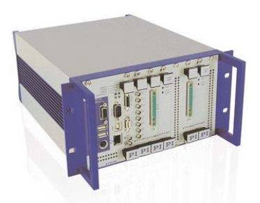
Figure 2. E-712 digital controller
The system also incorporates rapid spiral and sinusoidal areal scans into its command set, besides the NxM simultaneous gradient search capability. These scans are integrated with advanced fitting algorithms to precisely localize the centroid of general couplings such as quasi-Gaussian, top-hat and tilted couplings.
The E-712 digital controller is set off by high-speed fine and coarse XYZ stage stacks (Figure 3). Using this system, a standard full-field areal scan can be carried out within 400 to 600msec, and standard gradient search optimization can be completed within a matter of seconds for one-mode waveguide couplings on both output and input at the same time.
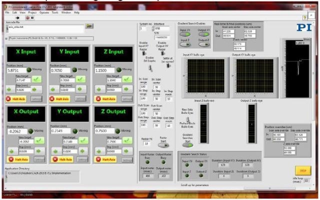
Figure 3. Pi consolidated coarse/fine XYZ alignment GUI
Example Tests
In order to demonstrate the capabilities of the E-712 system, particularly its fab-class coupling repeatability, rigorous testing was done on all its alignment modes including its concurrent waveguide output and input coupling optimization. Figure 4 shows some example test summaries.
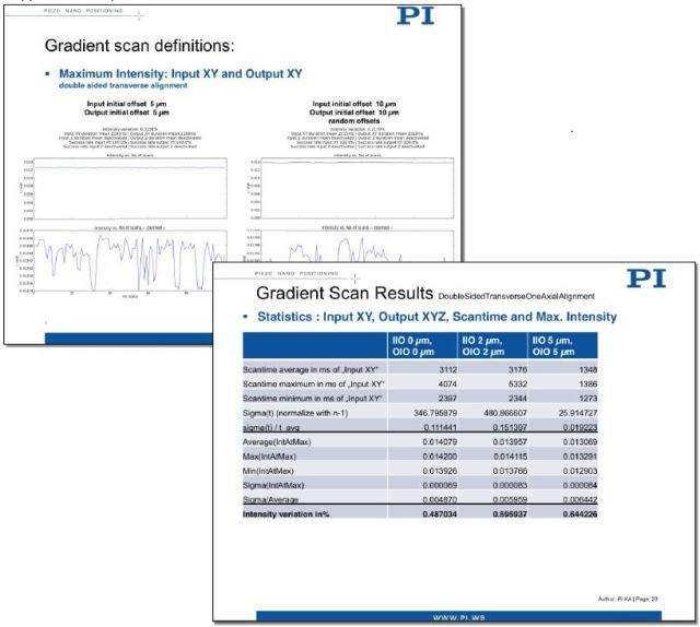
Figure 4. Example tests of the NxM technology
Besides the rapid alignment and continuous tracking capabilities, the E-712 system provides excellent reproducibility and stability. Since both fine and coarse axes are closed loop, the absolute position of all axes is known and controlled, thus removing the inherent creep common in open-loop nanopositioners. Likewise, the application of DC servomotors with high-precision encoders removes missed steps and heat-driven drift that may originate from implementations of stepper and motor.
Conclusion
The NxM technology integrated into PI's E-712 advanced digital controller provides high-speed TCP/IP, RS-232 and USB interfaces and a high-level mnemonic ASCII command set. This enables universal compatibility even with legacy fab automation PCs.
Moreover, advanced dynamic libraries that are compatible with Linux, Windows, and OS X computers promote rapid development of applications in different languages. A Windows LabVIEW library is also provided, in tandem with scriptable operation through Python and MATLAB platforms as well as compiled and source-code versions of an ActiveX- compatible GUI utility, which can perform quick, interactive input/output XY and Z optimization for waisted couplings.

This information has been sourced, reviewed and adapted from materials provided by PI (Physik Instrumente) LP, Piezo Nano Positioning.
For more information on this source, please visit PI (Physik Instrumente) LP, Piezo Nano Positioning.