In recent decades, there has been an increased desire to miniaturize electronics, which, in turn, has enhanced the demand for nano-electrical characterization methods.
It is crucial that an understanding of the local electronic material properties, such as conductance, local capacitance, dopant density and dielectric constant is acquired for research and development of the semiconductor and microelectronics industries.
The use of atomic force microscopy (AFM) technology has been central to correlating local electronic properties with topographical structures at the nanoscale.
Techniques including conductive atomic force microscopy (C-AFM) and Kelvin probe force microscopy (KPFM) open up the possibility to record measurements for local currents and electric surface potentials.
Scanning capacitance microscopy (SCM), on the other hand, maps the capacitance or local carrier density.
To uncover buried structures that are widespread in multilayered modern integrated circuits (ICs), scanning microwave microscopy (SMM) is especially good. These measurements are critical for applications in failure analysis, optimization of semiconductor manufacturing processes and the simulation of device performance.
Scanning Microwave Microscopy
SMM is a scanning probe measuring method that determines the interactions of a microwave between a sharp tip and the sample. The microwave reflection coefficient (S11 parameter) reflects the ratio between the power transmitted to the tip and the power received after being reflected at the tip-sample contact.
The S11 parameter is applied to understand the tip-sample microwave impedance. The microwave impedance generates information relative to the local capacitance that can be utilized to infer the dielectric constant and the dopant density.
One of the main drawbacks of SCM, a similar technique to SMM, is that dopant density measurements are generally qualitative and cannot be applied to materials other than semiconductors.
Alternatively, SMM can be employed to establish measurements for a range of materials, including dielectric materials and metals,1 since it does not only rely on the modulation of the depletion capacitance in the sample.
Moreover, SMM can function at much higher frequencies, producing improved sensitivity and the high-precision electronics facilitate calibrated and absolute measurements.
While extracting numerical data is analytically possible in SMM, in practice, calibration samples keep the experiment from quickly becoming overly complex.
A conventional SMM setup is comprised of a radio frequency (RF) wave source and a receiver working at a few GHz (Figure 1). In a pure S11 measurement, the transmitter and receiver both function on the same frequency, and only one primary tone (or frequency) is heard in the frequency spectrum.
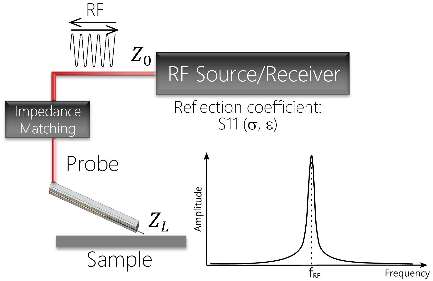
Figure 1. A schematic of a typical SMM setup: RF source/receiver electronics send the RF wave with impedance Z0 through the transmission line to the probe (red). The sample-probe impedance is ZL. The impedance matching circuit works as an “anti-reflection” medium between the low impedance Z0 and high impedance ZL. There is only one frequency peak (fRF) in the spectrum and the amplitude and/or phase are tracked during scanning of the surface. Image Credit: Nanosurf AG
A low-loss coaxial cable is used to transmit the signal to and from the cantilever. As the typical port impedance is 50 Ω and the tip-sample contact impedance is much greater, a corresponding circuit is usually necessary.
The RF electromagnetic wave starts radiating into free space once it leaves the coaxial cable. This can result in topographic cross-talk in the S11 measurement. In semiconductor materials, the S11 signal can be modulated by an AC voltage bias which modulates the dopant density in the sample under the tip.
Monitoring the change of S11 in relation to the switch of the bias voltage (akin to lock-in amplification) significantly reduces topographic cross-talk. This is known as the dS11/dV measurement, which produces information akin to the traditional dC/dV measurement in SCM. dS11/dV is only of use for semiconductors.
To attain this measurement, application of a low frequency (LF) modulation is carried out between tip and sample. The non-linearity in the tip-sample interaction results in frequency mixing between the RF and LF waves.
Thus, giving rise to sideband peaks on either side of the main tone (Figure 2).
The discovery of the sideband signal is conducted by mixing the signal back down to the LF frequency and demodulating it utilizing a lock-in or by directly measuring the amplitude and phase of the sidebands. The latter is the method of choice as it eliminates 1/f noise.
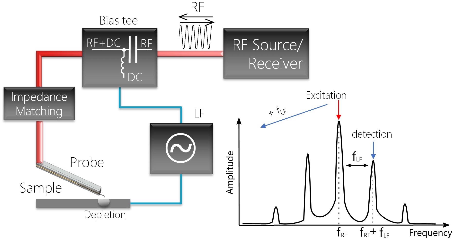
Figure 2. Schematic of a dS11/dV measurement: a low frequency bias voltage (LF) is applied between the probe and the sample. The non-linear behavior of the tip-sample contact causes frequency mixing between the RF and the LF signals. The frequency spectrum exhibits sideband peaks on both sides of the main RF tone (plot). The frequency of the mixed product, i.e. fRF+fLF, is used for detection of dS11/dV. Image Credit: Nanosurf AG
SMM Measurements
SMM applications include measuring dopant densities and failure analysis in semiconductor devices. An example of each is demonstrated below.
The S11 measurement of the Infineon SCM calibration sample and excellent contrast can be seen on dopant densities across the range of 1015-1020 1/cm3, as shown in Figure 3. The dS11/dV measurement offers supplementary data and the dopant kind (n or p) can be seen in the phase image.
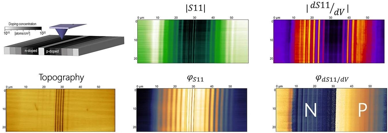
Figure 3. An S11 measurement (amplitude and phase) and a dS11/dV measurement (amplitude and phase) of an Infineon SCM calibration sample. Clear contrast between the regions of different dopant density can be observed in both the S11 and the dS11/dV measurements. The dS11/dV measurement indicates polarity and the type of the dopant (n or p) can be determined. The schematic image of the sample is taken from Ref. 2. Image Credit: Nanosurf AG
The SMM measurement raw data is uncalibrated, and the calibration process needs to be applied to the measured data to pull out quantitative values for the capacitance, resistance and material parameters. A comprehensive description of calibration procedures for SMM can be found in the relative literature.2,3
Another sample that shows structures with stark differences in dopant type and concentration is a semiconductor SRAM chip.
An SMM measurement of a device where relative changes in dopant concentration or device faults could be determined to assess the performance of the device or for potential sites for failure is displayed in Figure 4.
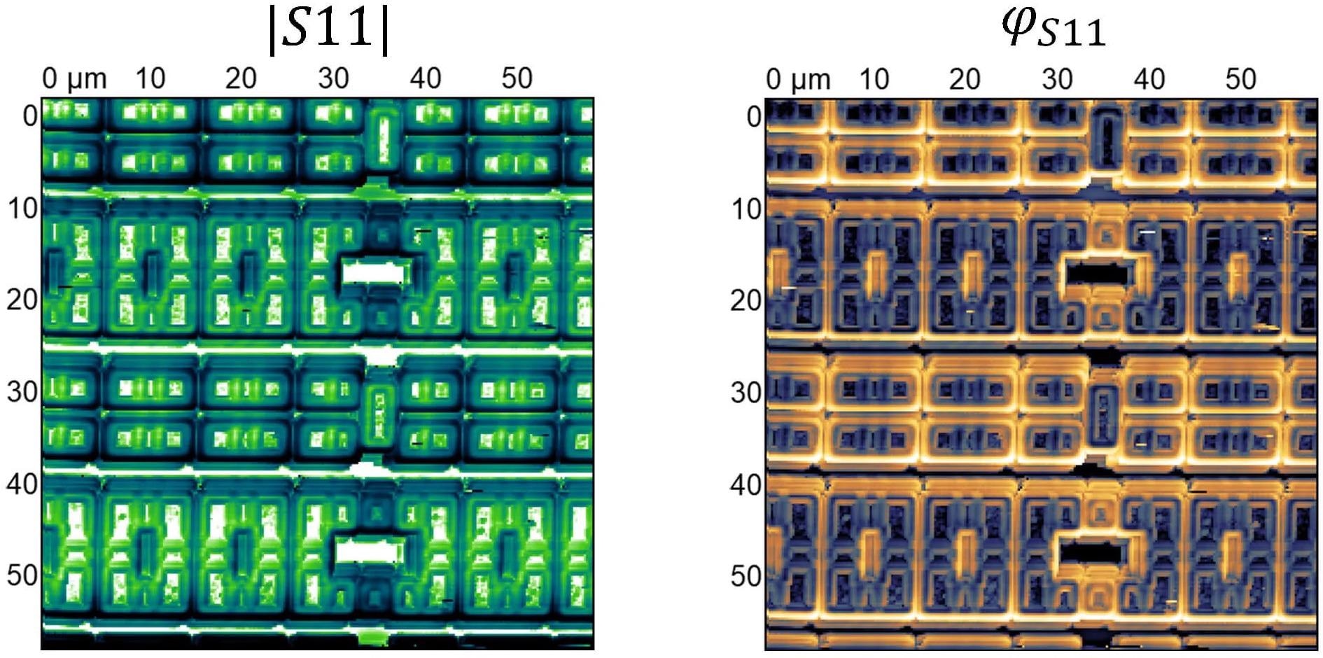
Figure 4. An S11 measurement (amplitude and phase) of an SCM sample, demonstrating high contrast between the areas of different doping levels. Image Credit: Nanosurf AG
Conclusion
SMM is a state-of-the-art alternative to SCM that does not solely depend on the use of resonant circuits to ascertain the S11 parameter or the microwave reflection coefficient measurements.
SMM can be applied to a range of materials that extend beyond semiconductors, including dielectrics and metals.
Calibration is not necessary for a number of critical applications, for instance, fault detection in the semiconductor industry. Still, when applying relatively simple calibration procedures, analytical calculations become possible, and material properties can be established quantitatively.
References
- J. Hoffmann et al., Appl. Phys. Lett. 105 (2014) 013102
- Brinciotti et al., Nanoscale 7 (2015) 14715
- Hoffmann J., et al., IEEE-NANO (2012)

This information has been sourced, reviewed and adapted from materials provided by Nanosurf AG.
For more information on this source, please visit Nanosurf AG.