Piezoelectricity is a material’s capacity to transform mechanical energy (pressing) into electric energy (polarization) and vice versa. The word “piezo” derives from the Greek word piezein, which means “to press tightly.”
The creation of electric polarization in response to applied stress is known as the direct piezoelectric effect. The directionality and the magnitude of polarization correspond to the stress applied, and the polarization can have elements in perpendicular and parallel directions.
In contrast, the inverse piezoelectric effect is the generation of a mechanical deformation as a reaction to an applied electrical field.
Piezoelectric materials are common in everyday life. For instance, ferroelectric materials are a subset of piezoelectric materials with an intrinsic spontaneous polarization and can be found in data storage, filters, nonvolatile memory, capacitors, thermistors, ultrasound imaging, oscillators, as well as light deflectors, monitors and modulators, to name a few.
Atomic force microscopes (AFM) are dependent on the inverse piezoelectric effect in their scanner design. As components are continually miniaturized in the electronics industry, piezoelectric thin films have also become a considerable area of interest (e.g., functionally coated flexible glass).
Thin films demonstrate piezoelectric behavior in specific regions (often called domains) in the sub-nanometer regime. Being able to comprehend the domain size as well as their response under an applied electric field allows for dynamic measurements of domain switching and local hysteretic behavior.
These material properties enable researchers to build an understanding of structure function relationships for material design. AFM can measure the local inverse piezoelectric response with greater fidelity and offer high-resolution piezoelectric information with correlative surface topography.
This mode of operation of AFM is often labeled Piezo response Force Microscopy (PFM). PFM can quantify deformations in the sub-nanometer regime and map ferroelectric domains with a lateral resolution of a few nanometers.
How does AFM work?
AFM is a surface characterization method where a fine needle is rastered at the free end of a cantilever across the sample surface. Light reflects back off the cantilever onto a position-sensitive photodiode that records the motion of the cantilever.
In PFM mode, AFM functions in contact mode where the cantilever is in persistent contact with the sample at a constant force. Thus, a sample is mounted on a conductive substrate, and a conductive cantilever is leveraged as the second electrode in order to apply an electrical field over the sample.
Each of the electrodes can be utilized to apply the voltage, though the first typically perform better. A schematic PFM setup is displayed in Figure 1.
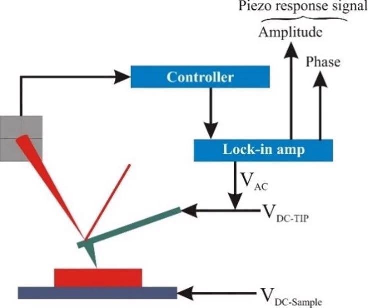
Figure 1. Figure 1: Schematic of a Piezo-response Force Microscopy experiment. Voltage is applied to a conductive tip in contact with sample and mechanical deformation of the sample is measured by the deflection of the laser. Image Credit: Nanosurf AG
To conduct measurements of the piezo response, an AC voltage is introduced between the tip and the substrate resulting in a periodic expansion and/or contraction of the sample.
With the tip in constant contact with the sample, the oscillatory movement of the sample surface instigates a periodic cantilever bending that is evaluated by the AFM controller’s lock-in amplifier.
Throughout PFM imaging, the amplitude and phase response of the cantilever are registered.
Phase contrast in PFM offers information in relation to the direction of the electrical polarization with respect to the electrical field. The amplitude indicates the magnitude of the piezo response and can typically be used to distinguish features such as the position of domain walls.
The components of electrical polarization can run parallel or antiparallel as well as perpendicular to the applied field. As shown in Figure 2, the AC field will produce out-of-plane and in-plane oscillations of the sample surface, hence resulting in vertical and lateral bending of the cantilever.
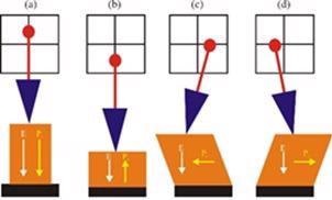
Figure 2. Schematics of (a-b) vertical and (c-d) lateral PFM mode. The applied electric field (E) and polarization (P) directions are denoted with arrows. Vector PFM is performed by combining data with a 0° and 90° rotation of the sample to obtain 3D vector information of the response. Image Credit: Nanosurf AG
If the response seen is simply parallel or antiparallel to the field (Figure 2a,b), the out-of-plane amplitude and phase of the vertical cantilever bending offer direct information regarding the magnitude and polarization (parallel vs. antiparallel) of the deformation in the sample.
Suppose the polarization and electric field are perpendicular to one another (Figure c,d). in that case, the result is the in-plane movement of the sample.
With a response that is purely out-of-plane, the effective piezoelectric coefficient, d33, can be determined from the measured amplitude (A) of the oscillation and the applied voltage over the sample (VAC):
d33=A/V AC
Below the resonance frequency of the cantilever, the amplitude A can be defined as pm (by conversion of voltage to distance utilizing the cantilever deflection sensitivity) and the effective piezoelectric coefficient can be quantitatively measured.
However, it is not as simple as comparing d33 measurements obtained by AFM with other bulk techniques. It is well established that material properties can significantly vary on the nanoscale in contrast to the bulk, and the piezoelectric effect is no exception.
In practice, materials can display a mechanical response across three dimensions. Movement both in-plane and out-of-plane in relation to the sample surface can arise as a response to the voltage applied.
To capture this, vector PFM is applied to track both vertical and lateral deflection of the cantilever. Moreover, a sample area is determined at two rotational orientations in relation to the cantilever. The data can be reconstructed mathematically for a combination of both the in-plane and out-of-plane vector components to create a 3D map of the piezo response.
Beyond imaging, AFM can also offer a good means to spectroscopy, writing domains with lithography or inducing polarization locally at the tip to better comprehend material hysteresis.
Experimental Setup
PFM requires an AFM with the ability to perform electrical measurements with conductive cantilevers, as shown in Figure 1. To measure both the out-of-plane and in-plane responses, two independent internal lock-in amplifiers are needed to measure each component’s phase and amplitude.
As shown in Figure 3, an additional and critical part for a number of samples is a camera view that enables a view of the sample from above to discern areas of interest. The location of the flakes of interest must be positioned beneath the cantilever, especially for 2D materials.
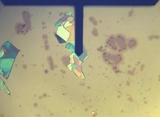
Figure 3. A top view camera image is essential for most PFM samples. This image shows flakes of 2D material on a gold substrate. Flakes of different thickness appear as different colors in the image. Image Credit: Nanosurf AG
There are numerous practical aspects of PFM that are worthy of mention, including cantilever choice and sample preparation. While flat samples are typically suitable for conducting PFM as standard, some rougher samples such as ceramics may necessitate polishing prior to imaging.
Caution should be exercised to ensure contamination-free surfaces. Generally, a thick insulating layer between sample and conductive substrate should be avoided, as this will diminish the field strength over the sample and hence the piezo response.
Conductive cantilevers for PFM come with an extensive range of force constants ranging from <0.1 N/m to =40 N/m with a resonance frequency range between 10-400 kHz.
Stiffer cantilevers reduce the contribution of electrostatic interaction with samples, whereas softer probes are less vulnerable to tip wear and sample damage when conducting scanning.
While it is possible to use Pt/Ir coated probes when conducting PFM measurements, studies have demonstrated that conductive diamond or PtSi coated tips have shown enhanced stability of the PFM signal.
Another crucial parameter for measurements is the optical sensitivity, which is inversely proportional to the probe length. Therefore, the shorter cantilevers offer a better signal.
Additional instrumentation is required for specialized PFM measurements such as high-voltage PFM (HV-PFM) and dual frequency response tracking (DFRT). For HV-PFM, an additional high-voltage amplifier is coupled with the user output of the AFM controller for direct control via the AFM software.
Calibration of the user channel is carried out so that the user can set the HV-amplifier’s output voltage directly. For this mode, it is possible to combine Nanosurf equipment with an external lock-in amplifier from Zurich Instruments, and signals can be imported via user input channels.
Zurich Instruments’ lock-in amplifiers are practical tools, not only for PFM, but other state-of-the-art AFM modes such as frequency modulated, heterodyne Kelvin Probe Force Microscopy (KPFM) and other multi-frequency applications.
Traditional PFM Applications
Lithium niobate (LiNbO3) is a dynamic ferroelectric material and is used extensively in applications that range from waveguides to piezoelectric sensors. A PFM measurement is displayed in Figure 4.
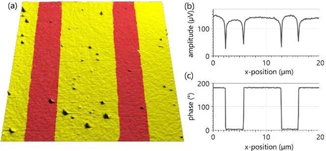
Figure 4. Vertical PFM images of periodically poled lithium niobate. (a) Representative topography with phase information color overlaid for a 20x20 µm2 area showing, (b) horizontal profile of the amplitude and (c) phase, showing little influence of amplitude with polarity and the 180° phase shift as expected. Data courtesy: Brian Odermatt, EPFL/Nanosurf. Image Credit: Nanosurf AG
This sample is poled periodically and demonstrates a pure out-of-plane response with alternating domains parallel and antiparallel to the applied field. Under ambient conditions, the piezo response is stabilized over an extensive voltage range of the applied electric field.
The topography and magnitude (amplitude signal) of the piezo response are not influenced by the polarization, but phase shifts by 180°, denoting a switch in the electrical polarization in the out-of-plane direction. The amplitude does not significantly change between the oppositely poled domains.
Ferroelectric 2D materials and thin films are attracting more and more interest with potential applications in electronics, energy and optoelectronics. PFM of CuInP2S6 flakes on a silicon substrate are displayed in Figure 5.
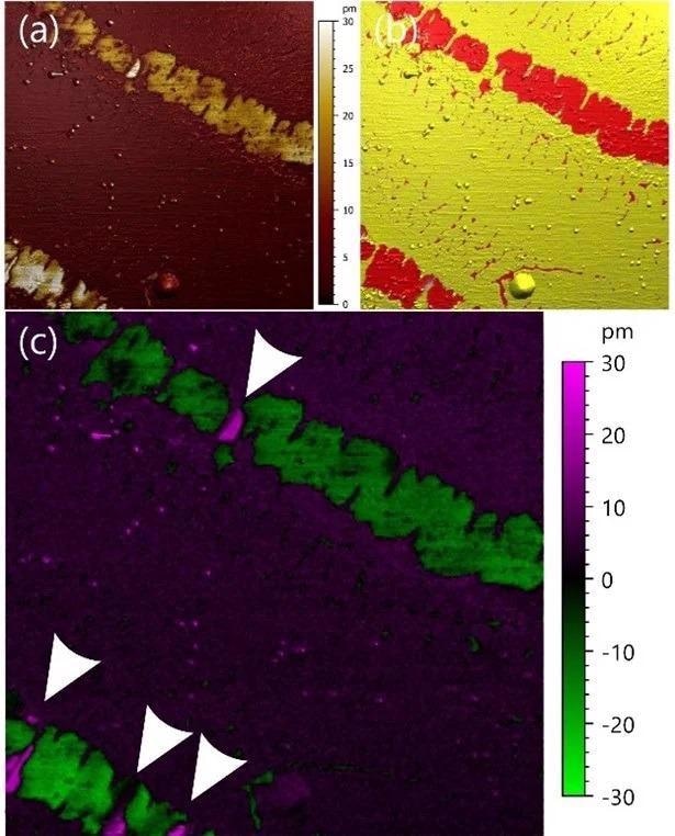
Figure 5. Vertical PFM imaging of 2D ferroelectric CuInP2S6 on Silicon substrate. (a) amplitude (b) phase and (c) amplitude projection, all represented as a color overlay on the topography. Image size: 5x5 µm2 (color scales do not include illumination effects from the topography visualization). Image Credit: Nanosurf AG
The magnitude of the vertical deformation (amplitude image, Figure 5a) and the equivalent polarization direction (phase image, Figure 5b) are indicated in the PFM measurements.
To distinguish the polarization direction of amplitude more easily, the amplitude and phase information can be brought together by applying an amplitude projection (Figure 5c).
By using the cosine of the phase, which is 0° or 180°, to multiply the amplitude, the sign remains consistent with the polarization direction, and specific domains can be observed more easily (Figure 5c, arrow heads).
Ferroelectric thin films can be characterized easily using PFM. Figure 6 displays the piezoelectric characterization of a piezoelectric and high magnetostrictive thin film that was grown on a flexible glass substrate using a sol-gel process.
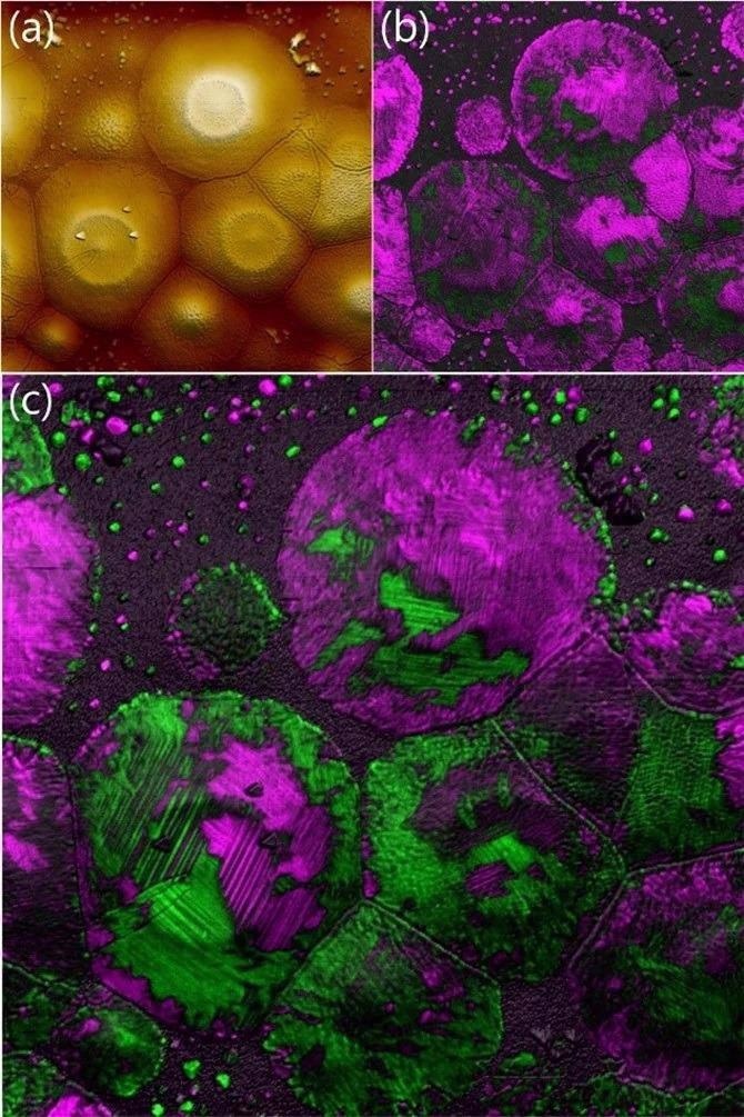
Figure 6. Out-of-plane and in-plane PFM response recorded on an 800 nm PZT thin film, grown by sol-gel method on Pt(111)/Ti/Flexible glass. (a) Topography, (b) out-of-plane amplitude projection, (c) in-plane amplitude projection. Image size: 9x9 µm2 (color scale do not include illumination effects from the topography visualization). Data courtesy: Dr. Itamar Neckel, Brazilian Center for Research in Energy and Materials – CNPEM, Brazilian Synchrotron Light Laboratory LNLS. Image Credit: Nanosurf AG
The surface topography shows “protrusions” with a dome-like morphology that are microns across (Figure 6a).
The amplitude projections of the out-of-plane response (Figure 6b) and the in-plane response (Figure 6c) clearly demonstrate the differences in domain size and structure within individual dome-like protrusions on the sample.
Dual Frequency Resonance Tracking (DFRT) PFM
In conventional PFM measurements, the probe oscillates at frequencies much lower than the resonance frequency of the cantilever (Figure 7a). One of the primary advantages of working at these frequencies is that the deflection can be easily converted into picometers, utilizing the deflection sensitivity of the cantilever.
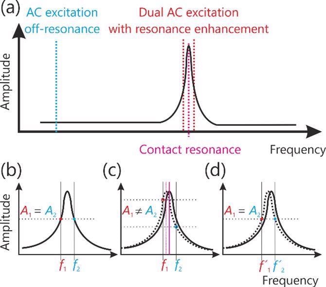
Figure 7. Schematics showing (a) traditional PFM measurement in off resonance mode and dual frequency resonance enhanced PFM mode. (b-d) DFRT amplitude response upon a change in contact resonance frequency. Image Credit: Nanosurf AG
However, signals are typically small, and measuring them can be a challenge, especially for thin samples.
The piezo response can be improved by working at a resonance frequency of the cantilever. Since PFM is conducted in contact mode, the first resonance frequency available is the contact resonance, where the cantilever produces a buckling movement with both the tip and the base of the cantilever fixed.
The sample is utilized as a “shaker piezo”, for oscillation of the cantilever in its (contact) resonance, which is about 4-5 times greater than the cantilever’s fundamental resonance frequency that is only fixed at one side.
Working at the contact resonance is vulnerable to crosstalk between the PFM response and other tip-sample interactions. This is due to the fact contact resonance is dependent on the local stiffness of the sample.
To prevent such crosstalk, the DFRT mode was introduced. In DFRT mode, the application of an AC voltage is carried out at two frequencies on either side of the contact resonance peak with the same amplitude (Figure 7b).
When there is a shift in the contact resonance, the amplitudes also experience a shift (Figure 7c), and a feedback algorithm in the lock-in amplifier neutralizes the difference by modulation of the excitation frequencies.
The difference Δf between the two excitation frequencies remains fixed in feedback (Figure 7d). Through the application of this method, variances in the contact resonance frequency are generally decoupled from the PFM response.
Contact frequency enhanced PFM can be applied for the study of the piezo-ceramic material - lead zirconate titanate (PZT). Improvement of fatigue and retention of PZT can be achieved by introducing tiny amounts of donor dopant-like ions of La3+.
With signal enhancement at the contact resonance frequency, grain and domain morphology, it is possible to examine the samples successfully with PFM, as shown in Figure 8.
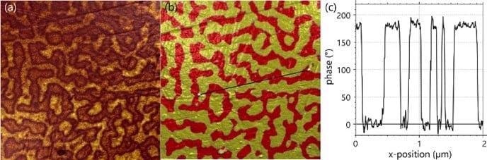
Figure 8. PFM measurement at contact resonance frequency (a) amplitude (arbitrary units), (b) phase (c) profile In the phase, showing domain widths ~100 nm range. Excitation: VAC= 5 V at f=304 kHz, Cantilever: Pt-coated Si with nominal spring constant k=1.5 N/m. Image size: 3x3 µm2. Sample courtesy: Prof. A. Kholkin, University of Aveiro, Portugal, data courtesy: Sergei Magonov, SPM labs, AZ. Image Credit: Nanosurf AG
As an example of DFRT, the PFM phase signal of a thin film of CuInP2S6 is displayed in Figure 9. In spite of a modualtion amplitude under 1V, the amplification by the contact resonance offers better contrast and presents clearer borders between oppositely polarized domains for better visualization.
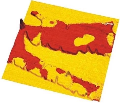
Figure 9. Piezo phase response from a thin film CuInP2S6 grown on a silicon surface imaged with DFRT PFM showing oppositely polarized domains while applying <1 V of AC modulation. Image Credit: Nanosurf AG
Spectroscopy and High-Voltage PFM
To look beyond imaging applications, AFM can also be utilized for spectroscopy and to locally “write” domains by subjecting the sample to a DC bias.
In spectroscopy, the amplitude and phase of the piezo response are quantified as a function of an applied bias voltage over the sample. One of the main applications for spectroscopy is to establish the voltage required for domain reversal.
In ferroelectric materials, the external voltage needed to reverse a polarization is known as the coercive field. To achieve the coercive field bias, voltages exceeding ±10 V may be required. In such cases, a high-voltage amplifier coupled to a user output for applying voltages up to ±200 V.
AC voltages can also be applied using the high-voltage (HV) amplifier to boost the signal-to-noise ratio of weak piezoelectric properties.
To conduct HV-PFM, the sample must be stable under high voltage. To avoid any physical harm coming to the user or subsequent damage to electronic equipment, caution must be exercised to ensure that no electronics are exposed when high voltages are applied.
However, an increase in bias voltage offset leads to an increase in the contribution of electrostatic forces on the cantilever. This electrostatic contribution may even surpass the PFM response, impeding domain reversal.
Switching spectroscopy PFM (SS-PFM) is a spectroscopy method to lessen the effect of electrostatics. Instead of ramping the voltage linearly, a train of voltage pulses is applied, switching off the voltage difference in between.
When switching, the AC voltage is applied continuously to record the PFM response both in the on and off states of the voltage.
This is depicted schematically in Figure 10. The “on” and “off” states represent the status of the DC bias voltage. While the DC voltage is applied to manipulate the polarization, the AC voltage is applied to simultaneously measure the piezoelectric signal.
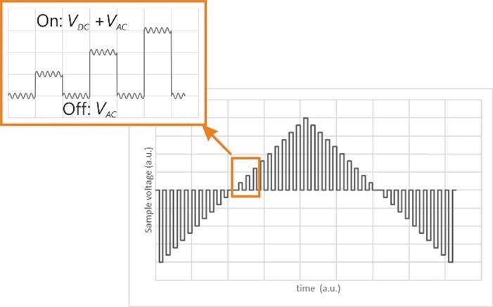
Figure 10. Schematic diagram of SS-PFM measurement depicting a train of DC bias pulses on top of an AC modulation. Image Credit: Nanosurf AG
The amplitude and phase behavior of a P(VDF-TrFE) thin film are demonstrated in Figure 11 to indicate SS-PFM. The data was registered during the off phase of an SS-PFM experiment. An HV amplifier was used to apply pulses between -40V and +40V.
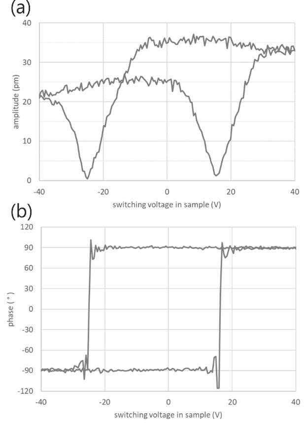
Figure 11. Piezo response hysteresis loop of P(VDF-TrFE) thin film (a) amplitude vs applied voltage and (b) phase vs applied volt-age obtained by SS-PFM. Sample courtesy: Joanneum Research Forschungsgesellschaft mbH, Austria. Image Credit: Nanosurf AG
As the voltage pulses were elevated, at +16 V, polarization switching was witnessed. This is signified by the amplitude dropping down to zero and the 180° phase shift. As the voltage was drawn back, the polarization switches back at -25 V, taking up a starting point.
Polarization and Lithography
Once the voltage required to overcome the coercive field has been established, for instance, from an SS-PFM experiment, the tip can be utilized to polarize the sample locally.
Lithography can be applied to write single domains, domain arrays and complex patterns without modifying the surface topography.
PFM high-voltage lithography on a P(VDF-TrFE) thin film is presented in Figure 12. The tip was biased and scanned in square regions to deliberately polarize regions and reverse the polarity of a smaller region.
A bias voltage of +40 V was applied to the sample substrate while a 3x3 µm2 area was first imaged.
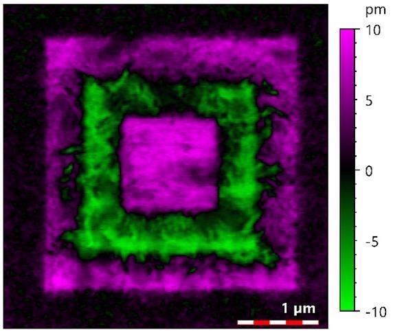
Figure 12. PFM amplitude projection of P(VDF-TrFE) thin film after applying DC sample bias of 40 V, -40 V, and 40 V during consecutive scanning of 3x3 µm2, 2x2 µm2, and 1x1 µm2 areas respectively. The AC amplitude amounted to 5 V. Sample courtesy: Joanneum Research Forschungsgesellschaft mbH, Austria. Image Credit: Nanosurf AG
Subsequently, the polarization was reversed by scanning areas of 2x2 µm2 and 1x1 µm2 and the application of -40 V and +40 V, respectively. Figure 12 displays a 4x4 µm2 image of the PFM amplitude projection (amplitude multiplied with the cosine of the phase) on the P(VDF-TrFE) film once these manipulation steps were completed.
Beyond the most prominent area, the polarization of the thin film does not occur, and as a consequence, the amplitude is small. After polarization with a positive substrate voltage, the sample demonstrates zero phase and high amplitude, indicated by the magenta color.
The 500 nm green region exhibits polarization reversal, with comparable amplitude, but opposite sign, as a result of the 180° phase difference. The magenta inner square is representative of a 1x1 µm2 region where the polarization was reversed for a second time.
It is interesting that the domain borders between the oppositely polarized regions stretch into the adjacent regions as it signifies a collective switching of domains beyond the tip-sample contact area.
Conclusion
Gaining an understanding of the piezo-responsive behavior of materials will remain central for the advancement of a broad range of technologies. As the miniaturization of electronics continues, characterization on the nanometer scale emerges.
Uniquely, PFM allows researchers to investigate the electromechanical properties of materials with nanometer spatial resolution and picometers of sensitivity.
The capabilities of Nanosurf PFM extend way beyond conventional PFM imaging to enhance the signal to noise, measure switching dynamics, conduct lithography and apply high voltages in line with experiment needs.
Notes:
- PFM is available on CoreAFM, FlexAFM and DriveAFM from Nanosurf.
- AFM and PFM images were processed with MountainsSPIP 9.

This information has been sourced, reviewed and adapted from materials provided by Nanosurf AG.
For more information on this source, please visit Nanosurf AG.