Due to the internet’s phenomenal growth, by 2025 the amount of data generated globally will be equivalent to a stack of DVDs that could circle the Earth 222 times or travel 23 times to the moon.1 The demand for data is already outpacing the capacity of current data storage solutions, which rely on magnetic or electric information stored independently in single-bit devices.
Due to this, it is now widely acknowledged that 4 bits (or even 8 bits) could be stored in a single cell memory device using technologies that can combine ferromagnetic and ferroelectric storage simultaneously.2
This represents a major improvement over single-bit technologies used today. Furthermore, the magnetoelectric multiferroics required for this technology enable energy-efficient electrical switching of magnetic memory states.3
Single-phase multiferroic materials are extremely uncommon in reality, especially at room temperature. By using the ferroelectric Aurivillius phase structure as a framework and chemically altering the composition to enable the inclusion of cations that drive ferromagnetic behavior within the same structure, scientists at Tyndall National Institute in Cork, Ireland, created a new layered-structured material.
Thin-film samples of B6TFMO (Bi6TixFeyMnzO18) with a clear ferromagnetic signature (remnant magnetization of 81.5 emu/cm3) at room temperature, in addition to the anticipated room temperature ferroelectricity, were successfully synthesized using both wet chemical (chemical solution deposition) and industrial-friendly (chemical vapor deposition) fabrication techniques.
Through this work, a rare single-phase multiferroic material that may be perfectly suited for the creation of new data storage devices was discovered for the first time.4–7
Using piezoresponse force microscopy (PFM), the Aurivillius phases were proven to be ferroelectrics for B6TFMO at the nanoscale. This method involves scanning a sample surface with a cantilever that has a pointed, conductive tip.
During contact mode imaging, applying an AC bias to the conductive tip causes the cantilever’s surface to move and deflect as a result of the opposing piezoelectric effect. The PFM amplitude images (Figure 1a) show the magnitude of the piezoresponse, and the PFM phase images (Figure 1b) display its orientation (0° or 180°).
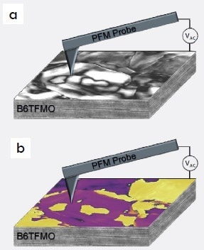
Figure 1. Schematic of the PFM technique showing PFM amplitude (a) and PFM phase (b). Image Credit: Asylum Research - An Oxford Instruments Company
By applying DC voltages to the nano-scale probes, the orientation of the ferroelectric polarization can be switched and arrays that demonstrate anti-parallel information storage states can be “written” into the material using the PFM lithography technique and retained, which is the basis for the active components of energy-efficient FeRAM capacitors (Figure 2).8
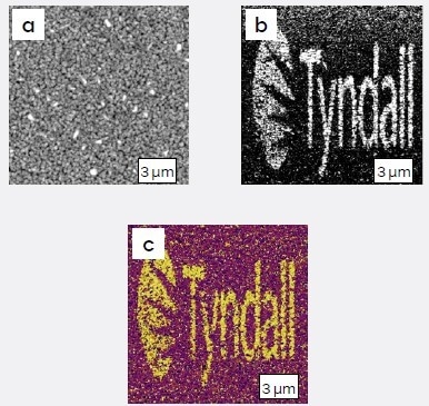
Figure 2. a) Topography, b) PFM amplitude and c) PFM phase images of Aurivillius phase thin film after patterning using the PFM lithography under 33.0 V DC bias. Image Credit: Reproduced from Journal of Applied Physics 112, 024101 (2012); https://doi. org/10.1063/1.4734983, Figure 11, with the permission of AIP Publishing. Image Credit: Asylum Research - An Oxford Instruments Company
These PFM measurements show that the material is ferroelectric, but it is also possible to look into its ferromagnetic properties. If multiferroic materials are also magnetoelectric, coupling between ferroelectric and ferromagnetic states allows data to be read and written using either electric or magnetic fields, reducing the amount of energy needed and increasing the materials’ technological potential.
By enabling PFM imaging in the presence of a controlled, variable magnetic field, the high voltage variable magnetic field module (VFM-HV) from Oxford Instruments Asylum Research made it possible to provide conclusive proof for magnetoelectric switching at the nanoscale.
By rotating a rare earth magnet to create the desired magnetic field, this equipment has a special design that prevents heating or drift as the field changes, allowing low-noise, highly accurate, spatially-resolved PFM measurements of the changing piezoresponse.
Direct PFM visualization of the nucleation, growth and switching of ferroelectric domains under the influence of a full in-plane magnetic field cycle (Figure 3) is shown in Figure 4.5 It is interesting to note that two different behaviors for magnetoelectric coupling were seen: irreversible switching and reversible switching.
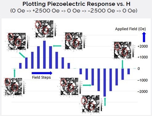
Figure 3. The cycled magnetic field used for the PFM images is in Figure 8. Image Credit: Asylum Research - An Oxford Instruments Company
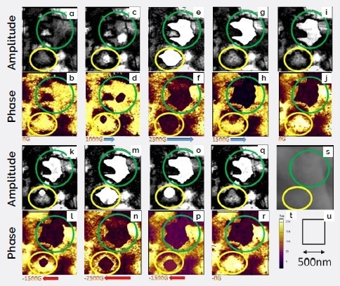
Figure 4. (a–r) Representative images of the effect of a complete magnetic field cycle (0 Oe -› +2500 Oe -› 0 Oe -› -2500 Oe -› 0 Oe) applied locally to the B6TFMO thin film sample on the in-situ out-ofplane (vertical) piezoresponse force microscopy measurements. (s) topography, (t) scale key for phase contrast, (u) scale key for sample area. The images demonstrate magnetic-field-induced irreversible (encircled green) and reversible (encircled yellow) ferroelectric domain nucleation (a and b), growth (c and d), saturation (e and f) under the magnetic field cycle. Taken from reference 5. Image Credit: Asylum Research - An Oxford Instruments Company
This demonstrates that the films are piezoelectric at ambient temperature and have zero magnetic fields. The green and yellow circles indicate new piezoelectric behavior that is seen when a magnetic field is applied.
The domain indicated by the green circle exhibits characteristics of irreversible magnetoelectric switching because it does not switch back when the magnetic field is reduced until it reaches zero. On the other hand, the vertical signal of the yellow-circled, piezoelectric domain vanishes, which is a sign of reversible magnetoelectric switching in the grains.
When the field is reduced to negative values, the reversible switching phenomenon is also visible. The nature of the magnetoelectric coupling in the polycrystalline B6TFMO thin films is likely to be influenced by the crystallite orientation concerning the direction of the magnetic field.
By creating ferroelectric hysteresis loops locally on the domains surrounded by green and yellow, it was possible to show how the magnetic field affects the vertical piezoelectric response in B6TFMO. By positioning the probe in a specific spot and applying a voltage profile, hysteresis loops are produced.
These allow one to calculate the voltage at which polarisation can change. The loops in Figure 5 show that the vertical piezoresponse increased for both types of domains as the magnetic field increased from +1000 Oe to +2500 Oe, which is consistent with the increase in vertical piezoresponse seen for the images above.
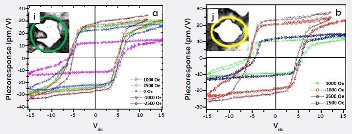
Figure 5. The effect of applied magnetic field on the piezoresponse force microscopy strain loops generated from (a) an irreversibly coupled domain shown in inset image (i) encircled green and (b) a reversibly-coupled domain shown in inset image (j) encircled yellow of the B6TFMO thin film sample. Taken from reference 5. Image Credit: Asylum Research - An Oxford Instruments Company
According to the piezoresponse images shown above, there was no difference in the vertical piezoresponse for the area circled in green for the loops produced at 0 Oe, −1000 Oe, and −2500 Oe changes in the magnetic field. On the other hand, reversible switching is illustrated for the yellow-circled area and the relationship between the strength and direction of the magnetic field and the size of the vertical piezoresponse cycles.
This study shows how an external magnetic field can activate an electric response and “switch” the polarization’s direction into its memory state. This occurs reversibly as the magnetic field cycles up and down for the areas circled in yellow.
Despite numerous reports of samples that display ferroelectric and ferromagnetic responses at room temperature, it has been established from earlier research9–11 that a thorough analysis of sample purity is necessary before one can be certain that a substance is a single-phase multiferroic.
Ferroelectric Aurivillius phase thin film samples, such as Bi5Ti3Fe0.7Co0.3O15 and Tb0.40Bi5.6Fe2Ti3O18, showed a distinct ferromagnetic signature in magnetic measurements. However, the results of a thorough investigation into the microstructure of the samples—including scanning transmission electron microscopy (STEM), high-resolution transmission electron microscopy (HRTEM), and energy dispersive spectroscopy mapping (EDS)—showed that these particular samples contained minute quantities of magnetic impurity inclusions, specifically CoFe2-xTixO4 (Figure 6) and FexTbyOz.
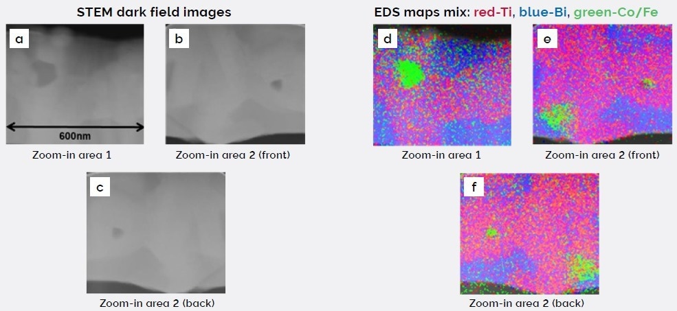
Figure 6. Cross-section analysis of Bi5Ti3Fe0.7Co0.3O15 in STEM dark-field imaging (a-c) and EDS mapping (d-f), Co (cobalt) rich inclusions are illuminated in green. As the lamella is electron transparent the Co rich areas can be easily identified from either side of the cross-section (b vs. c, and e vs. f). Image Credit: Asylum Research - An Oxford Instruments Company
This study emphasizes that magnetic responses that are observed in the main sample can be caused by secondary phase magnetic impurities, even when they are present in extremely low concentrations (like 0.01 vol%).
With analysis techniques like X-Ray diffraction (XRD), such trace levels of magnetic secondary phases are typically not detectable due to the noise level in any XRD scan placing a limit on the detectability (typically 1–3 vol%). Earlier studies on these kinds of materials lacked this level of in-depth analysis, which has influenced studies on the analysis steps that must be taken.
The B6TFMO samples were examined using EDS in conjunction with meticulous statistical analysis to examine phase purity. EDS is a method for determining a sample’s elemental makeup while it is being scanned by an electron beam. The method takes advantage of the fact that when an orbiting electron is displaced by an electron from the microscope beam, an X-Ray is produced.
The element is then identified through examination of the X-Ray energy, a fundamental property of an element. Multiple elements can be evaluated by an EDS detector at once because these X-Ray energies differ for various elements.
The composition of a material is characterized at a point, representing the interaction volume of the electron beam with the material, with the concentrations of the different elements present usually expressed in weight or atomic percent. As an electron beam scans across the sample surface, multiple points can be automatically analyzed to generate elemental maps that display the various elemental concentrations as a series of color-coded images.
Oxford Instruments' X-Max 80 EDS detector was used to collect elemental maps for the B6TFMO films. Numerous maps were procured across the entire film for statistical analysis, with differing detection limits and scanning areas.12 Undesirable second phase inclusions, like spinel-phase magnetite (Fe3O4) and other oxides, can be ferromagnetic, so their presence will produce a magnetic signature.
To find concentrations of all the magnetic elements that are present, scanning is required. However, the problem with these elements is that they are also present in the main phase, and the main phase ions will be responsible for most of the detected X-Ray signal for a given element. Slight variations in the Fe (iron) signal could only be seen by subtracting the Bi (bismuth) EDS signal from the summary EDS signal.
The filtered Fe EDS map (Fe signal minus Bi signal) for a map taken over 72 hours to boost the signal-to-noise ratio, attaining a detection limit of approximately 15 ppm in this case, is shown in Figure 7 to illustrate that point.4, 12
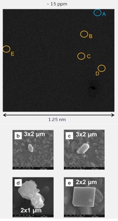
Figure 7. (Large image) Filtered Fe EDS map (Fe signal minus Bi signal) for a map taken over 72 hours achieving a detection limit of approximately 15 ppm. (Small images) Zoom-in SEM images of areas with increased Fe signal. Image Credit: Asylum Research - An Oxford Instruments Company
For the B6TFMO sample, Figure 8 displays colored elemental EDS maps overlayed on related STEM images. A brighter color denotes a higher concentration, and the magnetic elements [Fe or Mn (manganese)] are colored green. Yellow (small bright spot) and blue (circled) circles indicate two distinct types of areas with higher magnetic element concentration (large pale area).
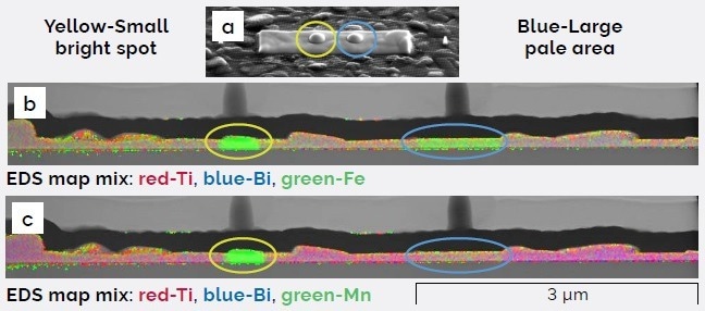
Figure 8. Color-coded mixed EDS maps overlain on their associated STEM images for the B6TFMO sample. Image Credit: Asylum Research - An Oxford Instruments Company
Further research was necessary because this concentration increase might be a sign of unwelcome second phase inclusions. These regions were discovered to be either non-ferromagnetic mangano-wüstite (Mn0.56Fe0.44O) or small grains of the primary Aurivillius phase, but with higher Fe concentrations, using TEM (Figure 9).
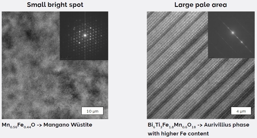
Figure 9. High-resolution TEM micrographs show the crystal structure of the 2 highlighted areas in Figure 8. This enabled the identification of the material phases in each area in conjunction with stoichiometry measurements by EDS in the cross-section. Image Credit: Asylum Research - An Oxford Instruments Company
With a confidence level of ≥99.5 %, this analysis and rigorous statistical analysis concluded that ferromagnetic impurities do not influencing the measurements taken.4 This is a crucial finding because one cannot be sure that a material is genuinely a single-phase multiferroic without such a thorough analysis of sample purity.
Memory storage cells made from multiferroic materials have the potential to increase the amount of information that can be stored by up to eight times.2 As a result, it is necessary to describe these materials in terms of their functionality.
Characterizing their chemical makeup is essential before this is done because the presence of secondary phase magnetic impurities can cause the material to exhibit a magnetic response. In this study, EDS was used to conduct a thorough chemical analysis of B6TFMO films. The results revealed that these unwanted impurities were not present, indicating that a single-phase multiferroic material had been created.
The ferromagnetic and ferroelectric response could then be characterized with certainty that impurity-free films had been created. It was demonstrated that B6TFMO samples show the reversible magnetoelectric switching required for real-world and energy-efficient device applications by possessing the unique ability to investigate piezoresponse under an applied magnetic field.
Moreover, since switching necessitates domain nucleation and growth, nucleation-limited ferroelectric domain switching can be tailored, and it is possible to design artificial nanosynapses in which the strength of the synapses changes with the amplitude and duration of the switching pulse.
In the pursuit of neuromorphic computing systems, the transformative technological possibilities of this multivalued logic will allow data processing using not only “yes” and “no,” but also “either yes or no” or “maybe” operations.
References
- ‘The Digitization of the World From Edge to Core’, An International Data Corporation White Paper – #US44413318 (2018); 2018.
- Yang, F.; Tang, M. H.; Ye, Z.; Zhou, Y. C.; Zheng, X. J.; Tang, J. X.; Zhang, J. J.; He, J., Eight logic states of tunneling magnetoelectroresistance in multiferroic tunnel junctions. Journal of Applied Physics 2007, 102 (4), 044504.
- Manipatruni, S.; Nikonov, D. E.; Lin, C.-C.; Gosavi, T. A.; Liu, H.; Prasad, B.; Huang, Y.-L.; Bonturim, E.; Ramesh, R.; Young, I. A., Scalable energy-efficient magnetoelectric spin–orbit logic. Nature 2019, 565 (7737), 35-42.
- Keeney, L.; Maity, T.; Schmidt, M.; Amann, A.; Deepak, N.; Petkov, N.; Roy, S.; Pemble, M. E.; Whatmore, R. W., Magnetic Field-Induced Ferroelectric Switching in Multiferroic Aurivillius Phase Thin Films at Room Temperature. Journal of the American Ceramic Society 2013, 96 (8), 2339- 2357.
- Faraz, A.; Maity, T.; Schmidt, M.; Deepak, N.; Roy, S.; Pemble, M. E.; Whatmore, R. W.; Keeney, L., Direct visualization of magnetic-field-induced magnetoelectric switching in multiferroic aurivillius phase thin films. Journal of the American Ceramic Society 2017, 100 (3), 975-987.
- Keeney, L.; Downing, C.; Schmidt, M.; Pemble, M. E.; Nicolosi, V.; Whatmore, R. W., Direct atomic-scale determination of magnetic ion partition in a room temperature multiferroic material. Scientific Reports 2017, 7 (1), 1737.
- Keeney, L., Schmidt, M., Amann, A., Maity, T., Deepak, N., Ahmad, F., Petkov, N., Roy, S., Pemble, M. E., Whatmore, R. W., Novel approaches for genuine single phase room temperature magnetoelectric multiferroics, (2016) in ‘Nanoscale Ferroelectrics and Multiferroics’, WILEY, Chapter 25, 789-829.
- Keeney, L., Groh, C., Kulkarni, S., Roy, S., Pemble M. E., Whatmore, R. W., Room Temperature Electromechanical and Magnetic Investigations of Ferroelectric Aurivillius Phase Bi5Ti3(FexMn1-x) O15 (x = 1 and 0.7) Chemical Solution Deposited Thin Films, (2012) Journal of Applied Physics, 112 (2), 024101.
- Keeney, L.; Kulkarni, S.; Deepak, N.; Schmidt, M.; Petkov, N.; Zhang, P. F.; Cavill, S.; Roy, S.; Pemble, M. E.; Whatmore, R. W., Room temperature ferroelectric and magnetic investigations and detailed phase analysis of Aurivillius phase Bi5Ti3Fe0.7Co0.3O15 thin films. Journal of Applied Physics 2012, 112 (5), 052010.
- Palizdar, M.; Comyn, T. P.; Ward, M. B.; Brown, A. P.; Harrington, J. P.; Kulkarni, S.; Keeney, L.; Roy, S.; Pemble, M. E.; Whatmore, R. W.; Quinne, C.; Kilcoyne, S. H.; Bell, A. J., Crystallographic and Magnetic Identification of Secondary Phase in Oriented Bi5Fe0.5Co0.5Ti3O15 Ceramics. Journal of Applied Physics 2012, 112 (7), 073919.
- Faraz, A.; Ricote, J.; Jimenez, R.; Maity, T.; Schmidt, M.; Deepak, N.; Roy, S.; Pemble, M. E.; Keeney, L., Exploring ferroelectric and magnetic properties of Tb-substituted m = 5 layered Aurivillius phase thin films. Journal of Applied Physics 2018, 123 (12), 124101.
- Schmidt, M., Amann, A., Keeney, L., Pemble, M. E., Holmes, J. D., Petkov, N., Whatmore, R. W., Absence of Evidence ≠ Evidence of Absence: Statistical Analysis of Inclusions in Multiferroic Thin Films, 2014 Scientific Reports, 4, 5712.

This information has been sourced, reviewed and adapted from materials provided by Asylum Research - An Oxford Instruments Company.
For more information on this source, please visit Asylum Research - An Oxford Instruments Company.