Sponsored by Nanosurf AGReviewed by Olivia FrostJan 13 2023
Surface roughness influences many mechanical properties, including friction and adhesion, surface reactivity, semiconductor substrate quality, and surface interaction with electromagnetic waves, notably ultraviolet (UV) light and X-Ray.
Therefore, a precise quantitative assessment of surface roughness is necessary to evaluate a surface’s functionality and appearance.
The most common roughness analysis method, published in the ISO 25178 international standard for measurement of 3D surface texture, calculates the root mean square (RMS) height (Sq) relative to the average height z̄ over an analyzed surface A.
 |
[1] |
Numerically, this corresponds to the total of all points on the surface
 |
[2] |
As shown by eq. 1 and the first part of eq. 2, roughness is dependent on the length scale. It is affected by the size of the analyzed area A and the lateral resolution Δx and Δy with which it is evaluated. The effective length scales are also influenced by any image processing applied to the images.
To correct for artifacts caused by a sample tilt or drift in z, it is common in AFM to remove a reference plane from the height data or apply a line-by-line flattening process to the images. Additional high-pass or low-pass filters can also be applied.
A high-pass filter eliminates the undulations of a sample, lowering the impact of features too close to the image size for accurate assessment. A low-pass filter removes features that are too close to the digital resolution and may cause digitalization artifacts.
To compare data, it is crucial to collect and analyze the data using the same set of measuring and processing parameters.
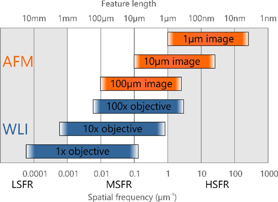
Figure 1. Spatial frequency bandwidth (SFB) accessible by WLI and AFM. Data digitization and image processing may affect the quantitative accuracy, particularly at ends of range. For AFM the image size is given in the graph and 512x512 pixels are assumed. With WLI 167 μm field of view is assumed for the 100x objective magnification and numeral apertures of 0.9, 0.25 and 0.04 for a 100x, 10x and 1x objective, respectively. Image Credit: Nanosurf AG
The length scale is characterized according to its inverse, the spatial frequency bandwidth (SFB). Low spatial frequency roughness (LSFR) targets lateral length scales above 1 mm, medium spatial frequency roughness (MSFR) addresses the length scale from 1 mm down to 1 µm, and high spatial frequency roughness (HSFR) handles the length scale below 1 µm.
The roughness of smooth surfaces decreases the sub-nanometer range in the MSFR and HSFR bandwidths, which is the domain for AFM measurements. The MSFR and, in particular, the HSFR roughness are important for ultra-flat surfaces used in EUV optical components for wafers and the semiconductor industry.
The formation of structures on wafers with dimensions of a few tens of nanometers requires a minimal surface roughness. Synchrotron radiation or EUV with wavelengths <15 nm is used for the production of such minute structures.
The optical elements used to illuminate wafers need not only a well-defined shape to provide a clean wavefront but also a low HSFR to lower the radiation’s unwanted scattering fraction R, which is dependent on the ratio between surface roughness Sq and wavelength λ.1,2
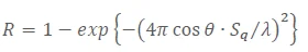 |
[3] |
With θ being the angle of incidence. Roughness values of 100 pm or below are required to bring down scattering adequately.3
White light interferometry (WLI) and atomic force microscopy (AFM) are two of the most commonly used methods for measuring such roughness levels. Figure 1 provides an approximation of the SFBs that are accessible using both strategies. WLI and AFM are highly complementary concerning the SFB, with a central overlap.
The SFB of WLI is restricted by the objective’s field of view and numerical aperture. It mostly spans the MSFR bandwidth, stretching into the LSFR for low-magnification objectives and into the HSFR bandwidth for high-magnification objectives. Therefore, WLI can reach length scales ranging from tens of millimeters to a few hundred nanometers.
The SFM of an AFM is restricted by the scan range of its scanner on the longer SFR side, the number of pixels, or the AFM cantilever tip radius towards the higher SFR. AFM scanner ranges generally extend to about 100 µm. At the upper end of the spatial frequency range, it reaches down to low-nanometer range features.
With scan sizes lower than 1 µm and a sufficient number of points, sub-nanometer lateral resolution can also be reached. Hence, AFM can access the HSFR and the higher-resolution portion of the MSFR.
The AFM offers a distinct advantage over WLI for analyzing the surface roughness of optical surfaces, particularly those with thin coatings. The mechanical probing of the AFM makes it exclusively reliant on upper-surface features, while reflected light from underlying layers can compromise the WLI’s roughness measurement of the top surface.
In this article, the main considerations for surface roughness analysis by AFM are demonstrated through the use of some examples.
Dependence of Roughness on System Specifications
System noise is one of the characteristics that can influence surface roughness that the AFM can measure. This is also known as AFM noise floor because it limits the minimum height change that can be detected. The system noise affects any measurement made by the AFM.
System noise levels of a few tens of picometers may be achieved with careful AFM and stage design, verification using finite element modeling (FEM), use of acoustic containers, and passive or active vibration isolation.
The system noise Ssys can be calculated directly from the variance in a height measurement on a surface without moving the cantilever laterally, yielding a zero scan size image. Surface features are therefore excluded from the measurement result.
Although the system noise influences the measured topography, it is usually safe to assume that the system noise is independent of the real topography. As a result, a more realistic value for the surface roughness can be determined by adjusting the measured roughness Sq,m values for system noise
 |
[4] |
This contribution quickly declines if the system noise is less than the measured noise. For instance, if a recorded RMS roughness of 90 pm is only 3x more than the system noise of 30 pm, the corrected roughness is Sq = 85 pm, which is roughly 6% less than the measured roughness.
This correction factor can still be greater than the measurement’s repeatability error and, therefore, should be included in the analysis.
AFM Design
The AFM design has a significant impact on the obtainable system noise. Many commercial AFMs fulfill this requirement for small samples. However, the samples are often bigger and heavier in the semiconductor and EUV optics industry, and the AFM requires translation axes to reach every position of the sample, either for random testing or at specific positions where defects have been found by other methods.
An AFM with a tip scanner is often needed because the (heavy) sample may be held stationary while the cantilever is raster scanned to capture the surface topography. The Nanosurf Alphacen system is an AFM platform that can process samples with side lengths ranging from 200 to 300 mm and can be equipped with sample chucks for typical wafers (4“, 8”, and 12” diameters).
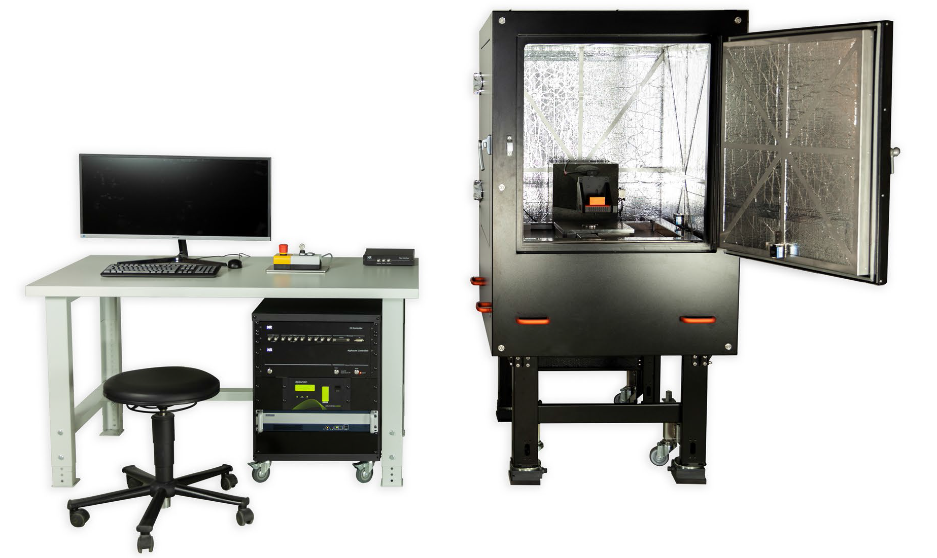
Figure 2. Alphacen tip scanning AFM, with a motorized stage providing full access to 300 x 300 mm2 large samples with weights up to 40 kg. The system is placed in an acoustic enclosure and includes active vibration isolation to reduce the effect of environmental disturbances. Image Credit: Nanosurf AG
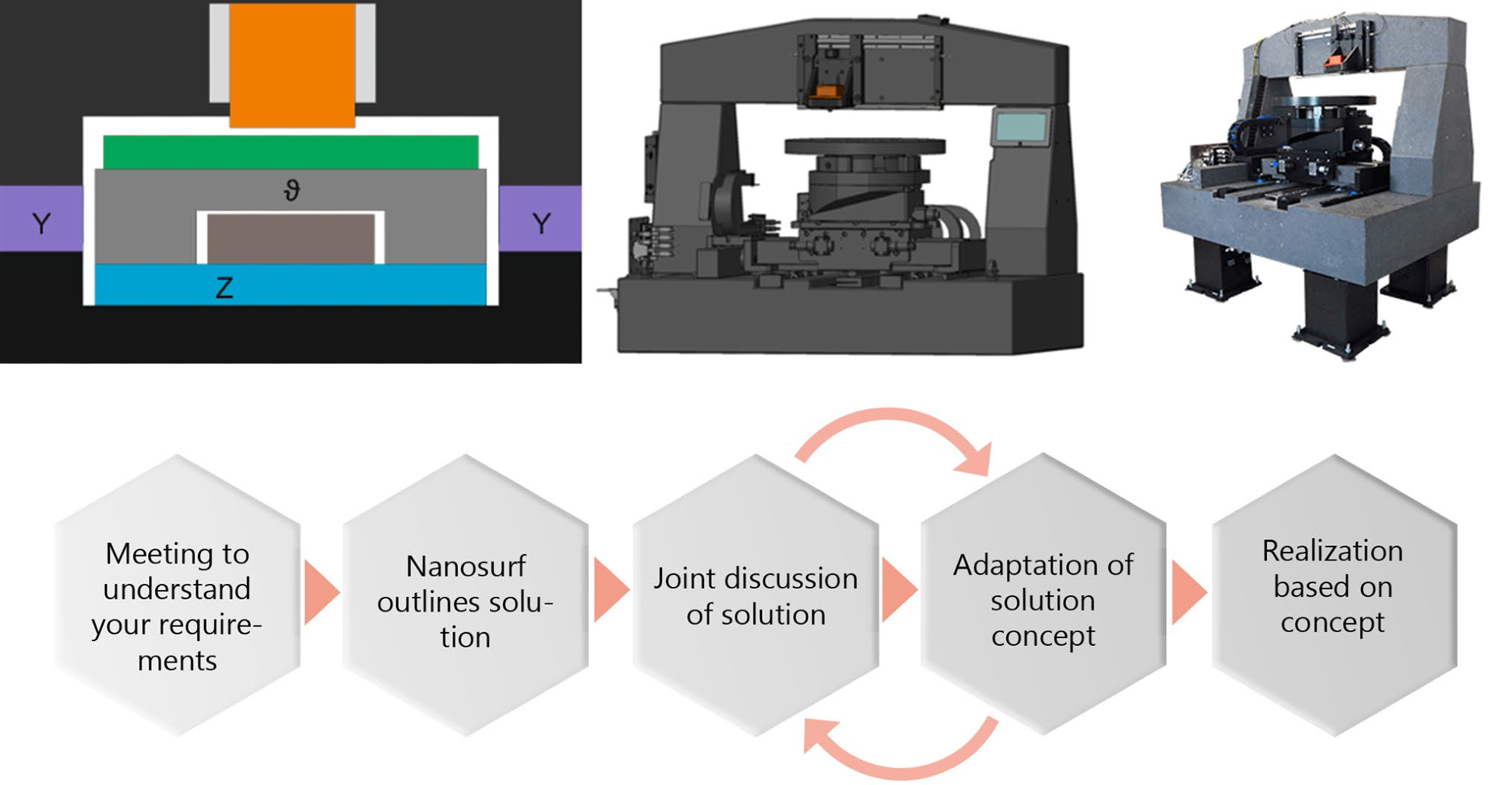
Figure 3. Design and realization process of tailor-made solutions for analysis of samples with geometries that cannot be handled by conventional AFM systems. Image Credit: Nanosurf AG
Access to the complete sample is provided through a stage concept with air bearings. Sample weights of up to 40 kg can be examined for roughness below 100 pm due to this stage design in conjunction with the AFM platform’s tip-scanning design.
Characterizing optical elements for surface roughness, common in semiconductor-related industries, presents some additional challenges. Optical elements may have convex or concave surfaces that can be either spherical, ellipsoidal, paraboloidal, cylindrical, or toroidal.
This requires tilting the sample or AFM scan head. Moreover, these samples may have a special mounting specification to ensure that the sample is not damaged on both the imaged side and its opposite side. To accurately measure sample roughness, the intrinsic system noise cannot exceed a few tens of picometers.
Samples must be examined in clean room settings for EUV, requiring the use of a cleanroom-compatible AFM and stage. Nanosurf collaborates with its clients and designs customized solutions for handling and measuring customer samples, as well as fulfilling all industrial regulations. To validate the design, FEM simulations are used extensively.
Tip Shape and Imaging Parameters
Surface roughness measurement is affected by the shape and sharpness of the AFM tip. A sharp tip that does not considerably convolute the morphology of the surface features is required for a precise quantitative assessment.
A blunt tip cannot accurately measure the features, leading to a widening of protruding and/or shortening of deep features. This causes incorrect measurements and an underestimation of the roughness.
Contact mode and dynamic mode are the two most popular imaging modes. In contact mode scanning, the tip is in constant contact with the surface. In dynamic mode, the cantilever oscillates at its resonance frequency or well below it (off-resonance tapping, ORT), and the tip occasionally taps the surface during the scanning process.
Dynamic imaging modes are most commonly used for roughness measurements in air. Contact mode has a more intense tip-sample interaction than dynamic mode and is more likely to dull the tip.
However, for certain very rough samples where the tip radius is less critical, contact mode imaging has the benefit of following the surface more reliably since it responds faster to the surface topography.
It is important to utilize soft imaging parameters to prevent tip wear. The tip-sample interaction is influenced by the imaging mode and parameters such as setpoint and scan. In contact mode, the setpoint is the force applied by the tip on the sample. The set point in dynamic mode is a user-specified fraction of the free air amplitude.
More demanding imaging settings, such as greater load or larger amplitude reductions, may hasten tip degradation. Scan speed is a variable that must be optimized once to evaluate the shortest possible time for capturing an image while preserving surface tracking and minimizing tip wear.
While tip wear is a prevalent issue when measuring roughness, tip contamination caused by imaging soft or sticky samples can also have a comparable adverse effect on roughness calculations.
The development of a consistent imaging parameters workflow is necessary for obtaining accurate roughness measurements using AFM. This involves sample preparation and cantilever definition in addition to the imaging parameters. Moreover, images must undergo similar post-processing procedures.
Applications
The Roughness of Glass and Fused Silica at Two Spatial Frequency Bandwidths (SFB)
Figure 4 shows images obtained on polished glass and fused silica, both with HSFR RMS roughness of less than one nanometer. Both samples were measured at two distinct SFBs with scan sizes of 15 x 15 µm2 and 1.5 x1.5 µm2 at 512 lines and 512 points per line.
This includes feature sizes ranging from 59 nm and 15 µm (0.067 µm-1 < SFB < 17 µm-1), or 6 nm to 1.5 µm (0.67 µm-1 < SFB < 170 µm-1), respectively. Each scan line was adjusted to remove low-frequency waviness by using a parabolic background subtraction.
The polished glass sample was slightly smoother than fused silica for the 15 µm image, with an evaluated roughness of 82±3 pm (Figure 4A), compared to 103±3 pm (Figure 4B). The higher roughness on fused silica corresponds to the features in the low micrometer length range that are absent on the polished glass sample.
In the 1.5 µm measurement, both surfaces showed comparable fine granular features that were not visible in the 15 µm image, with lateral dimensions between 6 nm and 60 nm. The roughness of the polished glass at 1.5 µm doubled in comparison to the 15 µm image (Figure 5C).
Figure 4. HSFR roughness on polished glass and fused silicon at two different images sizes. All images have been background-corrected line-by-line using a parabola function before the roughness analysis. Height range for all images: 1 nm. Image Credit: Nanosurf AG
The increase in roughness for the fused silica amounts to <10% (Figure 4D). The statistics show the frequency dependency of roughness measurements and the need to precisely define the appropriate measurement parameters. The significance of the roughness at each SFB may be different for different applications.
Repeatability of Roughness Values
To demonstrate the repeatability of roughness measurements, every sample from Figure 4 was examined 25 times. Figure 4 depicts the roughness of the polished glass and fused silica samples at two different scan sizes, as well as the system noise.
The measurement series was designed as 25 cycles of zero scan size, 1.5 µm scan size, and 15 µm scan size measurement, allowing for the detection of correlations between changes in each of the scan sizes by parameters such as tip wear.
The standard deviation for each set of 25 measurements was 5 pm or less, while the system noise readings were about 1.5 pm.
The correction achieved by eq. 3 of the observed RMS roughness for system noise is about 6% for the smoothest sample and less than 5% for the others, as shown in Table 1.
Except for the measurement with the greatest roughness, the adjustment is still more than the obtained standard deviation of the 25 measurements, indicating that this correction should be considered for system noise.
Repeatability with a standard deviation of less than 1 pm has also been obtained on proprietary samples.
Table 1. Table caption Repeatability overview of roughness measurements on polished glass and fused silica. Values are the averages and standard deviations of the system noise Ssys and measured RMS surface roughness Sq,m as shown in the figure, as well as the corrected value Sq using eq. 4. Source: Nanosurf AG
| |
Image size |
SFB |
Polished glass |
Fused silica |
| SSys |
0 |
- |
29.0 ± 1.5 pm |
31.1 ± 1.3 pm |
Sq,m
Sq |
15 µm |
0.067 µm-1 < SFB < 17 µm-1 |
82 ± 3 pm
77 ± 3 pm |
102.8 ± 1.1 pm
98 ± 2 pm |
Sq,m
Sq |
15 µm |
0.67 µm-1 < SFB < 170 µm-1 |
164 ± 5 pm
161 ± 5 pm |
161 ± 5 pm
106 ± 3 pm |
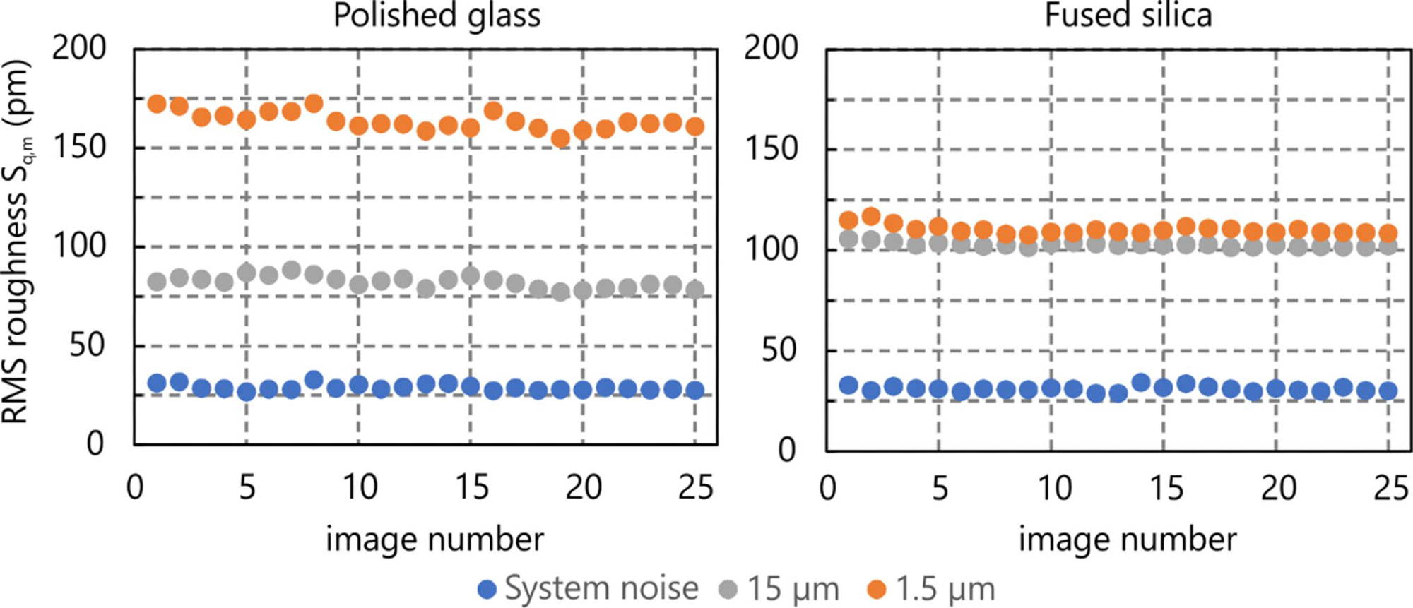
Figure 5. Repeatability of surface roughness measurements. 25 cycles were run, each containing height measurements with zero scan range (system noise), and scan ranges of 1.5 μm and 15 μm. Values are the measured RMS roughness values Sq,m after parabolic line-by-line background correction. Image Credit: Nanosurf AG
Roughness on Concave Samples
Tip-scanning AFMs provide increased measurement flexibility for non-flat samples. In the following example, a concave glass surface with a radius of curvature of 28 mm and a diameter of 30 mm was measured.
A reliable and compact method for accessing the complete sample can be created with a single lateral translation axis and two rotation axes perpendicular to the translation axis.
An example of a concave glass surface is shown in Figure 6. This sample is difficult to analyze with WLI because of its transparency and dielectric coatings.
The image depicts a variety of topographical features, such as pits and trenches. As a consequence, the height distribution is not Gaussian, making the interpretation of surface roughness more difficult. The measured roughness for the complete 20 x 20 µm2 image is Sq,m = 199 pm. However, it is heavily influenced by deep-lying features.
The evaluated roughness of a subarea without these topographic irregularities becomes Sq,m < 150 pm. The comparison of the roughness between the complete image and sub-image must be done with caution since the SFB is quite different for the two measurements.
Surface roughness analysis is complicated by irregular features such as pits, trenches, or protrusions. The resolution should be adequate to identify these features for reliable inclusion in the analysis.
The analyzed surface must have sufficient features to reach a level where their amount becomes indicative of the complete surface. For the example shown below, it is necessary to image multiple areas to obtain the average roughness and variation in roughness between different regions.
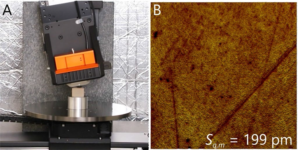
Figure 6. Roughness analysis of a concave surface an optical component with radius of curvature of 28 mm. A) AFM Setup with translation and rotation stage enabling the complete lens surface to be approached perpendicularly B) 20x20 μm2 image showing pits and trenches in the surface and exhibiting a roughness of 199 pm. Image z-range: 5 nm. Image Credit: Nanosurf AG
Other ISO25178 class roughness metrics can be used to characterize surfaces with irregular features. The skewness Ssk differentiates between protrusions and pits, whereas Sp and Sv give the highest and lowest points in an image, respectively.
Conclusion
The AFM is well suited to reliably measure roughness in the high spatial frequency range (HSFR), utilizing its high lateral and vertical resolution.
With unmatched resolution below 10 nm in the x and y-axis and <50 pm system noise in the z-axis, the AFM can detect 3D maps and surface roughness at the maximum spatial frequency range below 100 pm.
Many roughness metrics can be extracted from the data, the most popular being the standard deviation of heights (Sq). The AFM measurement is precise enough to allow the roughness to be corrected for the system noise.
When comparing roughness values across images or samples, it is essential that imaging parameters such as scan size and resolution are chosen carefully and that the parameters that influence the AFM tip-sample interaction be kept constant.
Finally, the noise floor of the AFM system must be lower than the sample’s roughness, which is essential for smooth samples.
Customized stage designs are required for analyzing large and non-flat samples that not only meet the requisite system noise specifications but also fulfill other requirements concerning safety or EUV compatibility.
References
- H. E. Bennett and J. O. Porteus, “Relation Between Surface Roughness and Specular Reflectance at Normal Incidence,” J. Opt. Soc. Am. 51, 123-129 (1961); https://doi.org/10.1364/JOSA.51.000123
- Sven Schröder, Tobias Herffurth, Angela Duparré, and James E. Harvey “Impact of surface roughness on the scatter losses and the scattering distribution of surfaces and thin film coatings”, Proc. SPIE 8169, Optical Fabrication, Testing, and Metrology IV, 81690R (30 September 2011); https://doi.org/10.1117/12.896989
- John S. Taylor, Gary E. Sommargren, Donald W. Sweeney, and Russell M. Hudyma “Fabrication and testing of optics for EUV projection lithography”, Proc. SPIE 3331, Emerging Lithographic Technologies II, (5 June 1998); https://doi.org/10.1117/12.309619

This information has been sourced, reviewed and adapted from materials provided by Nanosurf AG.
For more information on this source, please visit Nanosurf AG.