Sponsored by Nanosurf AGReviewed by Olivia FrostJan 18 2023
Over the past decade, demand for nano-electrical characterization has rapidly increased due to the continuous miniaturization of electronic devices.
The semiconductor and microelectronics industries rely heavily on the understanding of local electric material characteristics, such as conductance, dielectric constant, local capacitance, and dopant density.
Many methods have been developed to perform these measurements. These methods include conducting atomic force microscopy (C-AFM), Kelvin probe force microscopy (KPFM), and several electrical AFM modes for measuring local currents and potentials.
None of these techniques provide measurements of buried structures since modern integrated circuits are multilayered devices. Therefore, a technique that enables such subsurface imaging is essential for defect diagnosis and the optimization of manufacturing processes.
Scanning microwave microscopy (SMM) is a scanning probe method that integrates an AFM with the local tip-sample microwave impedance measurement, which is calculated using the S11 parameter or microwave reflection coefficient.1
The S11 parameter is a ratio between the microwave power delivered to the tip and the power returned after reflection from the tip-sample interface. A complex impedance measurement provides information about the local capacitance and resistance.
The dielectric constant and the dopant density in semiconductors may be calculated using local capacitance.
The SMM is very similar to scanning capacitance microscopy (SCM) in terms of the dopant density measurements. However, the SMM provides a broader range of measurements because it does not rely entirely on the modulation of the depletion capacitance in the sample. Therefore, it can be used for the assessment of both semiconductors and dielectric materials and metals.
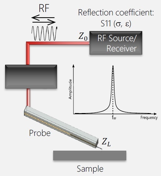
Figure 1. Schematic representation of a scanning microwave microscopy experiment. An RF signal is generated by the RF source and is being guided via a transmission line to a probe, which is in direct contact with a sample. The RF signal, reflected from the tip-sample contact with impedance ZL, travels back to the electronics via the same path and is being registered by the receiver. The ratio of the incoming and reflected waves is called S11 parameter, which is a function of local electrical properties of the sample, in the place of tip-sample contact. ZL is usually much larger than Z0 – the characteristic impedance of the transmission line, therefore a matching circuit is required to prevent full reflection of the wave. Excitation and detection frequency is the same – fRF (see inset). Image Credit: Nanosurf AG
SMM Technique
A conventional SMM setup includes a radio frequency (RF) wave generator and a receiver that operates in the few GHz range.
The wave generator and receiver are usually placed in the same housing and work on the same port. This provides the measurement of the S11 parameter, where the first and second indexes represent the number of the receiving and transmitting port.1
A transmission line, usually a low-loss coaxial cable, transports the signal to the cantilever. Due to the characteristic impedance of 50 Ω of the instrument and the much higher tip-sample contact impedance, there is also usually an impedance matching circuit between the tip and the instrument (Figure 1).
In an S11 evaluation, the transmitter and the receiver operate on the same frequency, and the frequency spectrum has only one major tone (demonstrated by the inset in Figure 1).
Microwave Basics
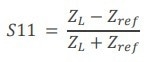
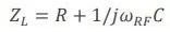
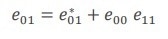
The S11 parameter is defined as a ratio between the difference and the total impedance of the load ZL and the reference Zref (Eq. 1):
 |
(1) |
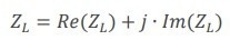
The reference impedance is typically 50 Ω, although, in most evaluations, it can be arbitrarily set as high as several kΩ. The load impedance is the tip-sample contact impedance and is a complex number with a real and imaginary part (Eq. 2), where j is the imaginary unit.
 |
(2) |
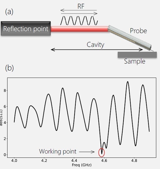
Figure 2. (a) Schematic representation of the reflection of an RF signal from impedance mismatch points and a corresponding frequency spectrum (b). The point in the spectrum with the lowest reflection is the natural working frequency for SMM. At this frequency smallest changes in tip-sample impedance would be the most noticeable. Image Credit: Nanosurf AG
The resistance is responsible for the real component of the impedance, whereas the inverse capacitance is responsible for the imaginary part (Eq. 3):
 |
(3) |
Working with microwave admittance instead of impedance is an alternate method of operation. In this case, the real component is conductance, and the imaginary component is capacitance. As a result of impedance being a complex number, the S11 parameter is also a complex number (Eq. 4):
 |
(4) |
Or in the polar coordinates (Eq. 5):
 |
(5) |
There are always two measured quantities in the S11 measurement, either the real and imaginary components or the amplitude and phase, and the calculations for extracting the sample parameters should be done using complex numbers.
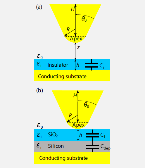
Figure 3. (a) Schematics of the parallel plate capacitor tip-sample geometry with an insulating film and conducting both tip and the substrate. Image adapted from Ref. 2. (b) Schematics of the tip-sample geometry in case of the semiconductor sample with the depletion capacitance Cdep and the parallel plate capacitor capacitance Ci connected in series. Image Credit: Nanosurf AG
If the Im (S11)(ωRF) function is shown at various capacitances using Eqs. 1 and 3, it becomes clear that the higher the ωRF, the lower the smallest detectable capacitance.
The tip-sample interface is a natural reflection site for microwaves because of its high impedance, and there are numerous reflection spots along the transmission line. These produce microwave resonator cavities, implying that peak and minima would exist on the S11 frequency spectrum (Figure 2).
The minima on this spectrum are selected as a working point for setting up the SMM measurement since this is where the S11 is the most sensitive to variations in the tip-sample impedance.
Capacitance Measurement
The SMM measurement is an impedance analysis with both resistive and capacitive components. The capacitance is often the most informative portion in many cases. In this section, the mechanism for the extraction of data from the tip-sample capacitance is demonstrated.
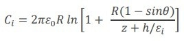
The first illustration shows the extraction of an insulating material’s dielectric constant. The capacitance of a parallel plate capacitor is dependent upon the dielectric between the plates. A thin film of an insulating material placed between the tip and a conducting substrate is considered a model for this example (Figure 3).
The dielectric constant of the insulator can be calculated from the capacitance data of such a setup using the following equation (Eq. 6):2
 |
(6) |
Where R is the tip radius, z is the tip height above the surface (zero when in contact), h is the thickness of the dielectric, and ωo and ωi are dielectric constants of vacuum and dielectric, respectively.
The analytical derivation of the dielectric constant from this measurement technique requires exact knowledge of the dielectric thickness as well as the conducting substrate.
However, researchers are often confronted with bulk portions of the dielectric material or dielectric films of unknown thickness. In these cases, the measurement must be calibrated with three well-established standards.3
SMM analysis of the dielectric constant spans the range between 1 and 1000 and is more precise than the electrostatic force microscopy (EFM) measurements.3
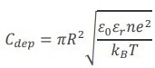
The carrier density in semiconductors is another common parameter that can be extracted from capacitance. In this example, the capacitance of relevance is the depletion capacitance of the semiconductor.
This capacitance may be in series with the capacitance of the parallel plate capacitor in a conventional sample (Fig. 3). The depletion capacitance varies with carrier density, as shown in Eq. 7:
 |
(7) |
Where ωr is the semiconductor’s dielectric constant, n is carrier density, e is the electron charge, KB is Boltzmann constant, and T is temperature. In this case, the equation for the total capacitance would be (Eq. 8):
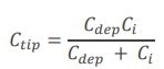 |
(8) |
The Cdep can only be extracted if Ci is known, and this is only feasible after the determination of insulator thickness. In controlled settings, washing away the oxide from the surface and growing a fresh layer is recommended.
Calibration Algorithm
Although analytical techniques may be used to derive sample parameters from SMM measurements, the calculations demand exact knowledge of the sample parameters and are computationally expensive.
In semiconductors, it is also vital to understand which model to apply for carrier mobility. In practice, calibrating the measurements against established standards4 is a considerably quicker technique for gathering quantitative data.
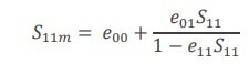
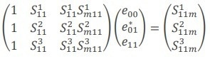
Figure 4 shows the algorithm of the calibration. The S11 measured at the port of the receiver S11m is not the same as the S11 at the tip-sample interface. The SMM connects these two observation planes and may be characterized using the three error variables.
The two planes and the error parameters are shown in the schematic on the left of Figure 4. The arrows on the schematic represent microwave propagation.
The e01 is responsible for the wave transmission from the source to the tip and back to the receiver, and the e00 and the e01 characterize the internal reflections at the port and tip, respectively.
The process begins by measuring three known impedances and constructing a linear system of equations using Maison’s rule (Eq. 9 - 11):
 |
(9) |
 |
(10) |
 |
(11) |
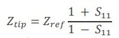
The system is non-linear and difficult to solve until the e01 is replaced by the product of e00 e11 and a new parameter e01.* After solving the system and determining the error parameters, the reverse operation can be applied to correct the measured S11m to find the S11 at the tip-sample contact (Eq. 12, 13):
 |
(12) |
 |
(13) |
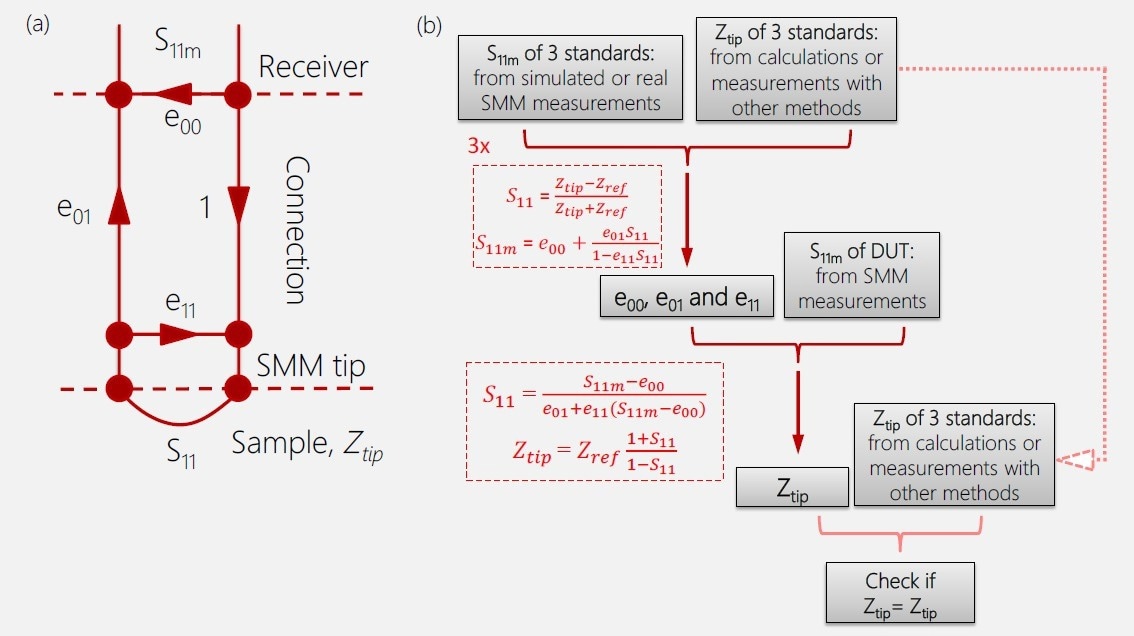
Figure 4. Calibration algorithm for extraction of tip-sample impedance from the S11 measurement. (a) Schematic representation of the with error coefficients and two different planes – the measurements plane of the receiver, and the plane of interest – between the tip and the sample. (b) The calibration algorithm, consisting of determination of error coefficients, and consequent calculation of the tip-sample impedance, using these error coefficients. Image Credit: Nanosurf AG
The resistance and capacitance may then be calculated from the Ztip using Eq. 3.
Calibration Example
Consider the capacitance calibration sample prepared by NIST and offered by MC2 Technologies as an example (Figure 5a). The sample is made up of silicon oxide terraces of varying heights and golden dots of different sizes deposited on these terraces.
The dots with varying diameters would have different capacitances, as would the dots with the same diameter but on terraces of varying heights.
To apply the algorithm to this sample, the capacitances of three dots highlighted with small red circles and indicated with numbers 1, 2, and 3 in Figure 5e must be analytically determined.
These calculations are done similarly to Eq. 6, but instead of the tip radius, the radii of the dots and the calculated values as Ztip from Eq. 13 are used.
In the calculation, the capacitance of two capacitors in series was taken into account. The top electrode of the first capacitor is made from a golden dot, whereas the bottom electrode is placed at the interface between the SiO2 and Si.
The second capacitor provides the depletion capacitance of the Si substrate. The total capacitance is then determined using Eqs. 7 and 8.
The capacitances were determined to be 0.3, 3.6, and 12.4 fF. The three S11 values needed for building the system of Eq. 10 are now calculated. The reference impedance (Zref) is taken as 10 kΩ.
Once the system has been solved and the error parameters have been determined, the algorithm is applied in reverse (Figure 4), and values of S11 for the complete image from the image of measured S11m are calculated.
The Ztip for the complete image is now determined, although it is mostly determined by the capacitance in this example (Figure 5e). The values of the calculated capacitances are in excellent agreement with the values of this sample determined by other groups.5
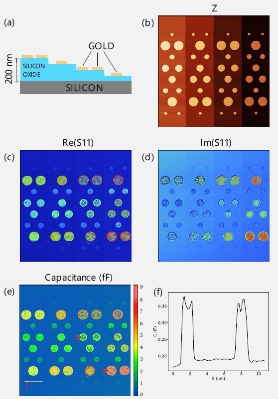
Figure 5. Example of calibration of S11 measurement of the MC2 Technology capacitance calibration sample. (a) Sample schematics showing 4 terraces, each 50 nm high, with patterned golden dots on top. (b) Topography of the sample, measured in contact mode. (c,d) Images of real and imaginary parts of S11 parameter. (e) Capacitance image, recalculated from the S11 parameter. Capacitors indicated with numbers 1, 2 and 3 were selected as calibration standards. Their respective capacitances were theoretically estimated as 0.3, 3.6 and 12.4 fF. These values vere used to calculate the capacitance map. (f) Cross section along the white line in (e), showing the contrast of a scan over two smallest capacitors. The smallest capacitance change in the image – the step between the terraces is 0.04 fF. Scan size: 52 x 52 μm2 . (b) Range: 0.43 μm. Image Credit: Nanosurf AG
Acknowledgments
The MC2 calibration capacitance sample was provided by LNE, France (Dr. Khaled Kaja and Dr. François Piquemal). Nanosurf would like to thank Dr. Johannes Hoffmann (METAS) for his successful discussions.
References
- https://en.wikipedia.org/wiki/Scattering_ parameters
- Gomila et al., J. Appl. Phys. 104 (2008) 024315
- Hoffmann et al., Appl. Phys. Lett. 105 (2014) 013102
- Hoffmann et al., IEEE-NANO (2012)
- F. Piquemal et al., Nanomaterials 11 (2021) 820

This information has been sourced, reviewed and adapted from materials provided by Nanosurf AG.
For more information on this source, please visit Nanosurf AG.