Sponsored by Nanosurf AGReviewed by Olivia FrostJan 18 2023
Scanning microwave microscopy (SMM) is a scanning probe method that uses the S11 parameter to calculate the local tip-sample microwave impedance. This impedance is affected by the sample’s local electrical characteristics, such as dielectric constant (ε), conductivity (σ), and carrier density (n).
These characteristics are critical in the design of semiconductor devices. Scanning Spreading Resistance Microscopy (SSRM) can also provide similar measurements, but this method generally uses diamond tips and high tip pressures to cut through a silicon oxide layer, which damages the sample surface. In addition, SSRM cannot differentiate between the n and p dopants in the sample.
The relationship between current vs. dopant density is non-monotonic, making the calibration of SSRM measurements extremely challenging. Scanning Capacitance Microscopy (SCM) is an alternate approach that suffers from similar difficulties while analyzing dopant type and density.
In this article, SMM was used to examine an Infineon silicon SCM calibration sample containing both n and p dopants and a range of dopant densities between 4⋅1015 – 1020 cm-3, with ten distinct density regions for each type (20 regions in total).
Figure 1 depicts a schematic of the sample. This sample has also been studied by different groups.2
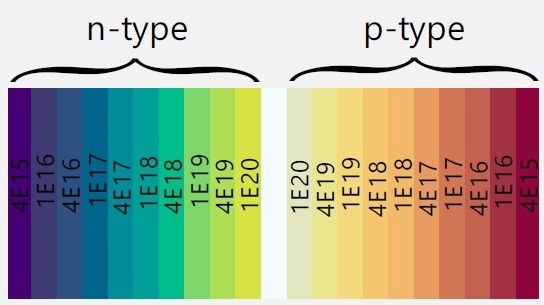
Figure 1. Schematic representation of a region of interest in an Infineon SCM calibration sample made of silicon. The area consists of 20 regions with different doping: 10 for each dopant type (n and p). With dopant densities in the range 4⋅1015 - 1020 cm-3. Exact dopant densities for each region are indicated in the sketch. The width of each line is 2.5 μm, the total width is of the area. Image Credit: Nanosurf AG
For sample characterization, two distinct SMM modes were used. The first method is the S11 measurement, in which the microwave signal has just one frequency for emission and detection. The second analysis method is called dS/dV measurement, which will be explained in further detail below.
dS/dV Measurement
The S11 measurement is susceptible to topography cross-talk because every change in height results in a change of cantilever sample capacitance.
In semiconductors, an AC voltage bias can change the dopant density of the sample beneath the tip, changing the S11 signal. This is known as the dS/dV measurement method, and it provides similar information to the typically used dC/dV measurement in SCM.
The dS/dV measurement method is less affected by topography, but it is only applicable to semiconductors. Another benefit of this approach is that it provides information about the type of dopants via phase change.
In the dS/dV case, low frequency (LF) AC voltage is supplied between the tip and the sample, and non-linearity in tip-sample interaction causes a frequency mixing between RF and LF waves, giving rise to sidebands (Figure 2).
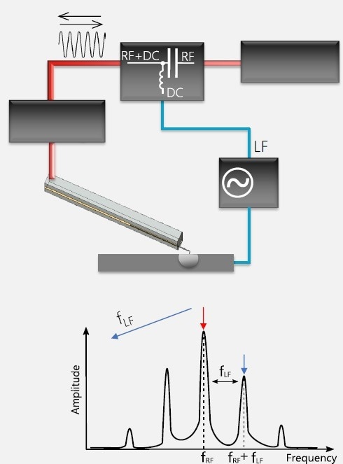
Figure 2. (a) Schematic of a dS/dV measurement: a low frequency bias voltage (LF) is applied between the probe and the sample. The nonlinear behavior of the tip-sample contact causes frequency mixing between the RF and the LF signals. (b) The frequency spectrum has now peaks on both sides of the main RF tone. The detector is working on the frequency of the mixproduct, i.e. fRF+fLF. Image Credit: Nanosurf AG
The signal detection on the sideband frequency can be achieved by several methods, such as down-mixing the signal to the LF frequency and measuring it using a lock-in amplifier. Alternatively, the receiver can also be adjusted to operate on a frequency a few MHz away, with digital mixing and filtering done on an FPGA.
The drawback of the dS/dV approach is the same as that of the dC/dV measurement; the signal amplitude is non-monotonic with the dopant density. Therefore, a combination of S11 and dS/dV measurements is recommended for a thorough analysis.
Theoretical Background
The measurement of tip-sample capacitance is the basis for determining dopant density in semiconductors via SMM (or SCM). This capacitance is made up of the metallic tip of the SMM, the oxide below the tip, and the semiconductor. It is a metal oxide semiconductor contact (MOS).
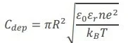
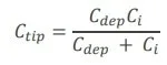
The tip-sample capacity is composed of the capacity Ci of tip and oxide in series with the semiconductor’s depletion capacitance Cdep. The depletion capacity forms when a voltage is introduced between the SMM tip and the semiconductor.
The applied electric field and charge carrier diffusion in the semiconductor cause depletion capacity. The electric field either attracts or repels electric charges from the surface, while diffusion opposes this force.3 This Cdep is a function of carrier density (Eq. 1):
 |
(1) |
In this case, the total capacitance equation would be (Eq. 2):
 |
(2)
|
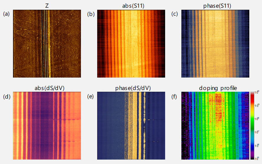
Figure 3. Experimental data of the S11 (b,c) and dS/dV (d,e) measurements of Infineon SCM calibration standard sample. The difference between the S11 and dS/dV can be clearly seen. The amplitude of S11 signal (b) is monotonically increasing with the carrier density, while the dS/dV signal (d) has largest amplitude in the middle of the range (1016-1018 cm-3 ). Phase signal of the dS/dV carries information about the type of dopants – n or p. The doping profile (f) was calculated from the S11 measurement (b,c). Image size (a,b,c,f): 50 x 50 μm2 , (d,e): 35 x 35 μm2. Image Credit: Nanosurf AG
The calibration protocol4 employed here is the same as the one used for the capacitance standard sample.1 However, in the previous case, the Cdep remained constant while the Ci varied due to the different sizes of gold dots.
In the current investigation, the Cdep was varied in different regions, and Ci was assumed to be constant across the measurement area, relying only on the tip size.
While tip dimensions are included in the calculations, the characterization of the tip can be avoided by using regions of “known” dopant densities.
Calibration Procedure
The S11 parameter measurement results and the dS/dV measurement of the Infineon SCM sample are shown in Figures 4a-e. For calibration, three areas in the sample were selected where the dopant density was assumed to be 1016, 4*1017, and 4*1019 cm-3.
The tip-sample capacitances were then calculated in these areas using Eq. 1-2, which were found to be 1.3, 3.4, and 4.7 aF, respectively, assuming a tip radius of 15 nm. The calibration protocol1,4 was used to evaluate the capacitance map of the complete scanning region.
The dopant density map was then computed from the capacitance map (Figure 4f). As seen in Figures 4b and 4c, the S11 measurement provides little information on the type of dopants. However, the phase of the dS/dV measurement may provide this information (Figures 4d and 4e).
Another distinction between the S11 and the dS/dV measurements is that, although the amplitude of the S11 signal increases monotonically from low to high dopant densities, the amplitude of the dS/dV reaches its maximum in the center of the density range (1016 – 1018 cm-3).
Conclusion
SMM measurement is an effective method for analyzing semiconductor samples. It provides useful information about carrier concentration and carrier type. However, S11 and dS/dV modes of SMM must be employed for a comprehensive examination.
References
- “Studies of MC2 capacitance standard sample by scanning microwave microscopy”, Application Note, Nanosurf AG (2022)
- Brinciotti, E, Nanoscale 7 (2015) 14715
- Wilson, P. R., Solid-State Electronics 12 (1969)
- Hoffmann et al., IEEE-NANO (2012)

This information has been sourced, reviewed and adapted from materials provided by Nanosurf AG.
For more information on this source, please visit Nanosurf AG.