Sponsored by MerckReviewed by Emily MageeJan 23 2024
Since its discovery back in 2004, graphene has attracted a great deal of interest due to its remarkable electrical conductivity, extensive surface-to-volume ratio, unique optical and vibrational properties, exceptional mechanical strength, and superb biocompatibility for potential use in biochemical sensing applications.1-4
The surface of graphene, marked by specific defects and chemical functionalities, also serves as an excellent reaction site for catalysis and electrochemical biosensing.5
This success has spurred exploration into similar materials like transition metal dichalcogenides (TMDs), transition metal oxides (TMOs), transition metal carbides/nitrides (MXenes), and hexagonal boron nitride (hBN) for biosensing applications.6,7
The diverse composition, structure, and functionality of these two-dimensional (2D) materials make them highly promising for developing innovative biochemical sensors. Additionally, the recent progress in the engineering of 2D materials via stacking, doping, functionalization, and alloying enables the construction of even more complex structures.
This article will briefly highlight recent progress in synthesizing and preparing 2D materials, focusing on their relevance in biosensing applications. It includes a summary of the most studied biosensors based on 2D materials, primarily electrochemical and optical biosensors (Figure 1).
It also explores lesser-explored biosensing technologies involving 2D materials. The article concludes with a look into the future of 2D materials as biomedical analytical tools and offers insight into where research is likely to go.
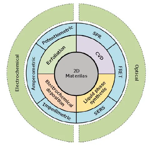
Figure 1. An overview of various synthesis methods (i.e., exfoliation, chemical vapor deposition (CVD), electrochemical deposition and liquid phase synthesis) of 2D materials for application in electrochemical biosensors (i.e., amperometric, potentiometric, and impedimetric methods) and optical biosensors (i.e. FRET: Forster resonance energy transfer, SERS: surface-enhanced Raman spectroscopy, and SPR: surface plasmon resonance). Image Credit: Merck
Synthesis of 2D Materials for Biosensing Applications
Preparation methods for 2D materials used in biosensors typically fall into several categories: mechanical and chemical exfoliation, electrodeposition, chemical vapor deposition (CVD), and solution-phase synthesis.
This section concentrates on the synthesis of 2D layers which leads to the production of 2D flakes, powders, inks, and films.
Exfoliation
Mechanical exfoliation (or micromechanical cleavage (MC), stands as the most frequently reported method for deriing 2D materials from bulk layered structures.1
While the quality of 2D flakes obtained through MC surpasses that of other techniques, its reliance on experimental skill and limited yield hinder its application for scalable device fabrication. Conversely, chemical exfoliation methods are suitable for large-scale synthesis of 2D flakes.8
The Li-intercalation and exfoliation method was developed to improve control over flake thickness and exfoliation yield when preparing MoS2 901187, 901867, 808652), TaS2, TiS2 (808717), WS2 (808806), ZrS2, NbSe2 (>808679), WSe2 (808822), Sb2Se3 (401196), Bi2Te3 (733482), and hBN (901349, 901410).8
While chemical exfoliation does exhibit high yields and efficient generation of 2D flakes, modifications of the 2D surface during exfoliation can introduce defects and impurities, and the co-existing single- and multilayered flakes are difficult to separate.
Chemical Vapor Deposition (CVD)
Chemical Vapor Deposition (CVD) stands as a common method for synthesizing high-quality 2D materials across extensive areas.
For CVD, carbon-based precursors are introduced into a furnace at high temperature, where they react and/or decompose to deposit carbon onto substrates such as Si/SiO2, transition metal catalysts (Cu, Ni), or sapphire to form single- or multi-layer 2D materials.
Experimental parameters, including temperature, pressure, and substrate conditions, can tune the quality, size, and thickness of the 2D materials.
For instance, graphene with a single or few layers covering a centimeter-scale area has been prepared on conductive substrates using this method. This graphene can then be transferred to insulator substrates for device fabrication.9
In addition, catalyst-free CVD graphene has been successfully synthesized directly on sapphire, a dielectric substrate. This approach eliminates the potential damage caused by the transfer process and enables the fabrication of devices on graphene that is directly grown on the substrate.10
Electrochemical Deposition
Electrochemical deposition provides an alternate cost-effective method for creating thin films of nanomaterials at low temperatures. Tuning the morphology, thickness, and properties of these films involves adjusting applied current, voltage, and deposition time.
Graphene and rGO films have been electrochemically deposited on various working electrodes for biosensing applications, as detailed later in this article.11,12
Films prepared from 2D nanosheet dispersions featuring abundant edges can be structured with other nanoparticles to enhance signal strength and improve sensor sensitivity.13 However, obtaining high quality and reproducibility remains challenging due to the aqueous surroundings and uncontrollable deposition process.
Solution Phase Synthesis
Finally, solution phase synthesis enables the production of gram-scale quantities of 2D materials with precise thickness under mild conditions and low temperatures. It also permits functionalization in either aqueous or nonhydrolytic media.
Recent advancements in solution-based methods have facilitated the synthesis of graphene,14 TMDs (like MoS2, MoSe2, WS2, and WSe2),15 and MXenes,16 ensuring controlled thickness and morphology with high yield and scalability.
Additionally, these methods enable the direct preparation of specific phases of 2D materials, such as 1T′ MoTe2,17 which might be challenging to access through other techniques.
2D Materials for Biosensing Applications
There is an exponential surge in reports detailing the use of 2D material-based biosensors for detecting various biological targets like neurotransmitters (dopamine, serotonin, etc.), metabolites (glucose, lactose, ascorbic acid, adenosine, etc.), inflammation markers (such as hydrogen peroxide and nitric oxide), proteins, nucleic acids, bacterial cells, and heavy metals.
The subsequent sections of this article will summarize recent biosensor reports using 2D materials for electrochemical (amperometric, impedimetric, and potentiometric, including field-effect transistors (FETs))18-21 and optical (like FRET,22 SPR,23 and SERS24) detection of these targets.
Electrochemical Sensors
Electrochemical sensors are often the favored choice for biochemical sensing, particularly at point-of-care applications, due to their high sensitivity, rapid response, cost-effectiveness, and straightforward readouts, aligning well with integrated circuit (IC) technology.
In the realm of electrochemical sensor development, 2D materials play crucial roles either as the primary sensing element (such as the working electrode or channel material) or as substrates for further modifications involving metal, metal oxide, or carbon nanostructures, biological enzymes, or other functional 2D materials.
While many electrochemical sensors operate through amperometric detection (i.e., measuring current changes at a specific potential applied to a working electrode), others rely on potentiometric detection (i.e., observing changes in surface potential) or impedance spectroscopy (i.e., analyzing impedance changes concerning applied frequency).
Amperometric detection encompasses various techniques like cyclic voltammetry (CV), linear sweep voltammetry (LSV), differential pulse voltammetry (DPV), and chronoamperometry.
For instance, Sun et al.18 utilized a nanocomposite electrode and DPV to concurrently detect dopamine (DA), ascorbic acid (AA), and uric acid (UA) in phosphate-buffered saline (PBS).
Their sensor was based on a nanocomposite of MoS2 nanosheets (901187, 901867) synthesized by Li intercalation, combined with electrodeposited AuNPs (741949, 752568, 808628) and deposited on a glassy carbon electrode (GCE).
The resulting sensor displayed impressive detection limits of 50 µM, 50 nM, and 50 µM and linear ranges of 0.05–100 mM, 0.05–30 µM, and 0.05–40 mM for AA, DA, and UA, respectively.
The research group demonstrated that creating a heterostructure of iron-sulfide with graphene enables highly sensitive and selective voltammetry detection of hydrogen peroxide, with a detection limit of approximately 0.1 nM and effectiveness across six orders of concentration range.
The response significantly varies depending on the type of graphene used, with FeS/CVD graphene structures performing better than FeS/n-type and /p-type epitaxial graphene layers.
The in situ ability to monitor oxidative stress induced by heat shock in E. coli cells was also showcased.25
In another study, Rakhi et al.19 created a nanocomposite by combining MXene Ti3C2Tx nanosheets with AuNPs for amperometric glucose detection. They immobilized the glucose oxidase enzyme (GOx) onto this composite, coated it with Nafion (Cat. No. 70160), and successfully detected glucose levels as low as 5.9 µM in PBS (pH = 7), within a linear range of 0.1–18 mM.
Given that typical blood glucose concentration values hover around ~5 mM, this sensor holds promise for practical applications. Even after two months of storage, the sensor retained 93% of its response at 3 mM, demonstrating its durability and long-term stability.
Potentiometric biosensors mainly employ FET-based sensors, garnering attention for detecting various analytes. Zhang et al.20 developed a solution-gated potentiometric sensor for detecting glucose in PBS, utilizing CVD-grown graphene (900415, 900443, 900445, 773719> and 773700) for both the gate and channel.
The gate electrode underwent modification with PtNPs (685453,771937) and GOx, initiating glucose oxidation and resulting in H2O2 production.
This H2O2 was then oxidized, effectively altering the gate voltage. This was indirectly used to determine the glucose concentration with a glucose detection limit of 500 nM, which is low enough for noninvasive detection in samples like saliva and sweat.
Impedimetric sensors rely on changes in either Faradaic or non-Faradaic impedance in the presence or absence of a target analyte.
For the Faradaic detection of Salmonella, Jia et al.21 developed a composite of rGO/MWCNTs, electrodeposited onto a GCE. Once the electrode was prepared, they drop-cast an amino-modified Salmonella aptamer onto the electrode.
Based on the change in charge-transfer resistance, they were able to detect as few as 25 colony-forming units (cfu) per ml, with a linear range of 75–7.5 105 cfu/ml, in 60 minutes without any pretreatment.
Considering that the infective dose for typhoid fever-causing Salmonella can be as low as 1,000 cells, this sensor could find application in clinical settings.26
Optical Sensors
2D materials possess unique optical and vibrational properties alongside their tunable electronic and electrochemical attributes. These properties, such as photoluminescence, fluorescence quenching, second harmonic generation, and enhanced electron-photon interaction, make them well-suited for optical sensor applications.22-24
Various common optical sensing techniques, including Forster resonance energy transfer (FRET),22 surface plasmon resonance (SPR),23, and surface-enhanced Raman spectroscopy (SERS),24 are employed in this field. For instance, sensors utilizing fluorescence quenching or enhancement, like FRET, can detect alterations in the fluorescence presence/absence of a target analyte.
Kong et al. developed a sensor for prostate-specific antigen (PSA), a crucial marker for prostate cancer.22 They used Li-intercalated MoS2 nanosheets with a modified single-stranded (ss) DNA probe that exhibited fluorescence changes upon the presence of PSA.
In the absence of PSA, the fluorescence was strongly quenched, but upon the addition of PSA, the fluorescence returned. They reported a dynamic response range of 0.5–300 ng/ml, with a linear range from 0.5–60 ng/ml.
The limit of detection was 0.2 ng/ml, and the technique was selective in the presence of other common interfering proteins, including carcinoembryonic antigen (CEA). Since PSA values of 4 ng/ml or higher can be indicative of prostate cancer, this has obvious practical implications.
SPR sensors detect alterations in local refractive index when a target analyte is present or absent, leveraging the sensitivity of surface plasmons. 2D materials, owing to their thin film nature, significantly enhance the sensitivity of SPR sensors.
Kamaruddin et al.23 combined chitosan with graphene oxide (763705, 763713, and 777676) and deposited it onto an Au/Ag/Au layered substrate for detecting Pb2+ and Hg2+ ions.
Using the Kretschmann configuration, they detected less than 1 ppm for both ions, showing slightly higher sensitivity to Pb2+ ions than Hg2+ in linear regimes (2.05 and 0.29 °ppm-1 for Pb2+ and 1.66 and 0.20 °ppm-1 for Hg2+).
Apart from fluorescence-based and SPR methods, SERS can also be used to identify tiny changes in Raman scattering caused by analyte adsorption on surfaces.
For myoglobin (Mb, M0630, M5696) detection, Shorie et al.24 designed a SERS-based sensor that combined liquid-exfoliated WS2 nanosheets with AuNPs. Elevated Mb levels hint at muscle damage and can aid in the early detection of heart attacks.
This sensor employed an anti-Mb aptamer on the surface for selective Mb detection and could detect as little as 10-2 pg/ml, well below blood level values (~85 ng/ml), indicating heart attacks or muscle damage. The WS2/AuNPs combination yielded an enhancement factor of 6.78 x 10⁶.
Conclusions and Perspectives
This article offers an overview of recent strides in synthesizing 2D materials, focusing on their application in biosensing technologies. It delves into the pros and cons of various synthesis methods used to create 2D materials as biosensing platforms.
The unique properties of these materials enable innovative electrochemical and optical biosensors capable of detecting neurotransmitters, metabolites, proteins, nucleic acids, bacterial cells, and heavy metals.
With their exceptional sensitivity, ultra-thin structure, and adaptable functionalization, these materials have the potential to revolutionize healthcare, particularly in point-of-care diagnostics and flexible or transient bioelectronics.
However, to fully capitalize on their potential, further technological advancements and a deeper understanding of their properties are needed.
First, developing cost-effective synthesis methods for environmentally stable 2D materials and heterostructures with precise morphological control will enhance their compatibility with biosensing, especially on flexible platforms.
Second, understanding and controlling factors like layer number, defect chemistry, and material phase are crucial, given their impact on the sensing performance of 2D materials.
Third, exploring controlled functionalization of 2D material surfaces, which significantly influences their optical, electronic, and vibrational properties, represents an emerging area for research.
Lastly, it is vital to systematically investigate the biocompatibility and antibacterial properties of various 2D materials, beyond the commonly studied ones like graphene, GO, rGO, and MoS2, and their relation to the synthesis process.
References
- Novoselov KS. 2004. Electric Field Effect in Atomically Thin Carbon Films. Science. 306(5696):666-669. https://doi.org/10.1126/science.1102896
- Lee C, Wei X, Kysar JW, Hone J. 2008. Measurement of the Elastic Properties and Intrinsic Strength of Monolayer Graphene. Science. 321(5887):385-388. https://doi.org/10.1126/science.1157996
- Liu K, Zhang J, Cheng F, Zheng T, Wang C, Zhu J. 2011. Green and facile synthesis of highly biocompatible graphene nanosheets and its application for cellular imaging and drug delivery. J. Mater. Chem.. 21(32):12034. https://doi.org/10.1039/c1jm10749f
- Hendry E, Hale PJ, Moger J, Savchenko AK, Mikhailov SA. Coherent Nonlinear Optical Response of Graphene. Phys. Rev. Lett.. 105(9): https://doi.org/10.1103/physrevlett.105.097401
- Wang Y, Li Z, Wang J, Li J, Lin Y. 2011. Graphene and graphene oxide: biofunctionalization and applications in biotechnology. Trends in Biotechnology. 29(5):205-212. https://doi.org/10.1016/j.tibtech.2011.01.008
- Li Z, Wong SL. 2017. Functionalization of 2D transition metal dichalcogenides for biomedical applications. Materials Science and Engineering: C. 701095-1106. https://doi.org/10.1016/j.msec.2016.03.039
- Luo Y, Li Z, Zhu C, Cai X, Qu L, Du D, Lin Y. 2018. Graphene-like Metal-Free 2D Nanosheets for Cancer Imaging and Theranostics. Trends in Biotechnology. 36(11):1145-1156. https://doi.org/10.1016/j.tibtech.2018.05.012
- Zeng Z, Yin Z, Huang X, Li H, He Q, Lu G, Boey F, Zhang H. 2011. Single-Layer Semiconducting Nanosheets: High-Yield Preparation and Device Fabrication. Angew. Chem. Int. Ed.. 50(47):11093-11097. https://doi.org/10.1002/anie.201106004
- Kim KS, Zhao Y, Jang H, Lee SY, Kim JM, Kim KS, Ahn J, Kim P, Choi J, Hong BH. 2009. Large-scale pattern growth of graphene films for stretchable transparent electrodes. Nature. 457(7230):706-710. https://doi.org/10.1038/nature07719
- Fanton MA, Robinson JA, Puls C, Liu Y, Hollander MJ, Weiland BE, LaBella M, Trumbull K, Kasarda R, Howsare C, et al. 2011. Characterization of Graphene Films and Transistors Grown on Sapphire by Metal-Free Chemical Vapor Deposition. ACS Nano. 5(10):8062-8069. https://doi.org/10.1021/nn202643t
- Chen L, Tang Y, Wang K, Liu C, Luo S. 2011. Direct electrodeposition of reduced graphene oxide on glassy carbon electrode and its electrochemical application. Electrochemistry Communications. 13(2):133-137. https://doi.org/10.1016/j.elecom.2010.11.033
- Liu M, Chen Y, Qin C, Zhang Z, Ma S, Cai X, Li X, Wang Y. Electrodeposition of reduced graphene oxide with chitosan based on the coordination deposition method. Beilstein J. Nanotechnol.. 91200-1210. https://doi.org/10.3762/bjnano.9.111
- Zhang Y, Zeng GM, Tang L, Chen J, Zhu Y, He XX, He Y. 2015. Electrochemical Sensor Based on Electrodeposited Graphene-Au Modified Electrode and NanoAu Carrier Amplified Signal Strategy for Attomolar Mercury Detection. Anal. Chem.. 87(2):989-996. https://doi.org/10.1021/ac503472p
- Yan X, Cui X, Li L. 2010. Synthesis of Large, Stable Colloidal Graphene Quantum Dots with Tunable Size. J. Am. Chem. Soc.. 132(17):5944-5945. https://doi.org/10.1021/ja1009376
- Mahler B, Hoepfner V, Liao K, Ozin GA. 2014. Colloidal Synthesis of 1T-WS2 and 2H-WS2 Nanosheets: Applications for Photocatalytic Hydrogen Evolution. J. Am. Chem. Soc.. 136(40):14121-14127. https://doi.org/10.1021/ja506261t
- Naguib M, Gogotsi Y. 2015. Synthesis of Two-Dimensional Materials by Selective Extraction. Acc. Chem. Res.. 48(1):128-135. https://doi.org/10.1021/ar500346b
- Sun Y, Wang Y, Sun D, Carvalho BR, Read CG, Lee C, Lin Z, Fujisawa K, Robinson JA, Crespi VH, et al. 2016. Low-Temperature Solution Synthesis of Few-Layer 1T??-MoTe2 Nanostructures Exhibiting Lattice Compression. Angew. Chem. Int. Ed.. 55(8):2830-2834. https://doi.org/10.1002/anie.201510029
- Sun H, Chao J, Zuo X, Su S, Liu X, Yuwen L, Fan C, Wang L. 2014. Gold nanoparticle-decorated MoS2 nanosheets for simultaneous detection of ascorbic acid, dopamine and uric acid. RSC Adv.. 4(52):27625. https://doi.org/10.1039/c4ra04046e
- Rakhi RB, Nayak P, Xia C, Alshareef HN. 2016. Erratum: Erratum: Novel amperometric glucose biosensor based on MXene nanocomposite. Sci Rep. 6(1): https://doi.org/10.1038/srep38465
- Zhang M, Liao C, Mak CH, You P, Mak CL, Yan F. 2015. Highly sensitive glucose sensors based on enzyme-modified whole-graphene solution-gated transistors. Sci Rep. 5(1): https://doi.org/10.1038/srep08311
- Jia F, Duan N, Wu S, Dai R, Wang Z, Li X. 2016. Impedimetric Salmonella aptasensor using a glassy carbon electrode modified with an electrodeposited composite consisting of reduced graphene oxide and carbon nanotubes. Microchim Acta. 183(1):337-344. https://doi.org/10.1007/s00604-015-1649-7
- Kong R, Ding L, Wang Z, You J, Qu F. 2015. A novel aptamer-functionalized MoS2 nanosheet fluorescent biosensor for sensitive detection of prostate specific antigen. Anal Bioanal Chem. 407(2):369-377. https://doi.org/10.1007/s00216-014-8267-9
- Kamaruddin N, Bakar AA, Mobarak N, Zan MS, Arsad N. Binding Affinity of a Highly Sensitive Au/Ag/Au/Chitosan-Graphene Oxide Sensor Based on Direct Detection of Pb2+ and Hg2+ Ions. Sensors. 17(10):2277. https://doi.org/10.3390/s17102277
- Shorie M, Kumar V, Kaur H, Singh K, Tomer VK, Sabherwal P. 2018. Plasmonic DNA hotspots made from tungsten disulfide nanosheets and gold nanoparticles for ultrasensitive aptamer-based SERS detection of myoglobin. Microchim Acta. 185(3): https://doi.org/10.1007/s00604-018-2705-x
- Ebrahimi A, Zhang K, Dong C, Subramanian S, Butler D, Bolotsky A, Goodnight L, Cheng Y, Robinson JA. 2019. FeSx-graphene heterostructures: Nanofabrication-compatible catalysts for ultra-sensitive electrochemical detection of hydrogen peroxide. Sensors and Actuators B: Chemical. 285631-638. https://doi.org/10.1016/j.snb.2018.12.033
- Food and Drug Administration. 2012. Bad Bug Book, Foodborne Pathogenic Microorganisms and Natural Toxins. 2nd ed.

This information has been sourced, reviewed and adapted from materials provided by Merck.
For more information on this source, please visit Merck.