Materials are at the heart of every technological advance, from aerospace engineering to semiconductor devices. Understanding how they respond to mechanical stress is essential for designing stronger, more durable, and more efficient systems.
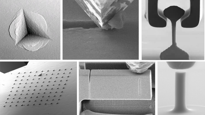
Image Credit: Alemnis AG
While traditional mechanical testing has long been the standard approach, an increasing number of researchers and engineers are now turning to in-situ micromechanical testing within scanning electron microscopes (SEMs) to gain deeper, more detailed insights.
Conventional mechanical testing provides bulk material properties, effectively averaging out the behavior of microscopic features like individual grains, interfaces, and phase boundaries. However, materials rarely fail uniformly at the macroscopic level. Instead, failures often stem from localized phenomena occurring at the micro- and nanoscale.
By scaling down testing dimensions, it becomes possible to study these localized effects directly - leading to better-informed decisions around material design and processing.
Micromechanical testing techniques, such as nanoindentation, make it possible to investigate small-scale deformation mechanisms, fracture processes, and strain localization. This approach is especially valuable for evaluating thin films, coatings, and advanced materials, where mechanical behavior can differ significantly from that of bulk counterparts.
The ability to test individual grains or specific microstructural features is opening up new possibilities in fields like metallurgy, additive manufacturing, and nanotechnology.
As miniaturization continues across industries such as watchmaking, micromechanical engineering, and microelectronics, testing methods must operate at even smaller scales than the components themselves to guarantee precision, reliability, and performance.
Berkovich nanoindentation map displaying imprints across carbides and matrix in steel, illustrating microstructural variations in deformation response. Image Credit: Alemnis AG
Conducting micromechanical tests in-situ (e.g., inside an SEM) adds a new dimension to materials analysis. Unlike traditional ex-situ methods, where tests are performed separately and only post-mortem analysis is available, in-situ SEM testing facilitates real-time observation of deformation with high spatial resolution.
The benefits include:
- Direct Observation of Failure Mechanisms: Researchers can visually track crack initiation and propagation, dislocation movement, and interface interactions under stress instead of relying solely on force-displacement curves.
- Targeted Testing: SEM imaging allows for precise positioning, enabling tests on specific microstructural features like grain boundaries or thin films.
- Correlating Mechanical and Microstructural Data: By synchronizing mechanical testing with high-resolution imaging, researchers can link stress-strain behavior with structural changes in real-time, enhancing understanding of material performance.
Progress in microfabrication techniques also enables the creation of customized samples for more complex mechanical testing, including micro tensile tests and nanotribology. These capabilities broaden the scope of material characterization, allowing for more precise assessments relevant to real-world applications.
The ability to analyze materials at the microscale in real time is reshaping multiple industries by providing critical insights into how materials perform under various conditions.
In aerospace and automotive engineering, it allows for the evaluation of lightweight alloys and composite materials, particularly under extreme environments where strength and durability are essential. In electronics and semiconductor devices, researchers can closely examine the reliability of thin films, solder joints, and MEMS components - ensuring these intricate systems maintain functionality and longevity.
For biomedical applications, microscale testing helps uncover the mechanical behavior of implants and biomaterials, ensuring they perform effectively within the human body.
In the energy and coatings sectors, microscale analysis is crucial for evaluating wear resistance, adhesion, and fracture mechanics in protective coatings and structural materials, ultimately improving performance and extending service life in demanding environments.

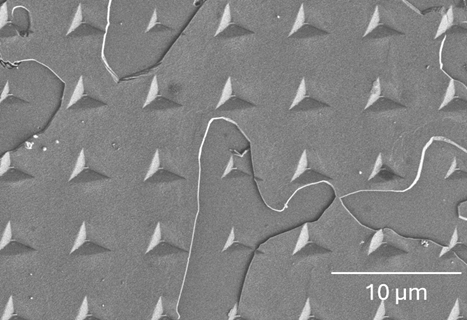
Micropillar compression of cemented carbide (WC-Co composite), revealing deformation mechanisms within WC grains and the Co matrix. Courtesy of Aalen University (Germany). Image Credit: Alemnis AG
From engineering stronger transportation materials to improving biomedical implants and advancing semiconductor reliability, real-time microscale material analysis is pushing innovation across a wide range of industries.
A natural next step in the evolution of in-situ micromechanical testing is evaluating materials under conditions that closely replicate their real-world environments. This includes high-temperature testing above 1000 °C, which is critical for assessing thermal stability, creep behavior, and phase transformations in aerospace and energy applications.
On the other end of the spectrum, low-temperature testing down to -150 °C provides vital insights for materials used in cryogenic environments, where ductile-to-brittle transitions can significantly affect performance.
Materials also often operate in liquid environments, such as biomedical implants exposed to bodily fluids or mechanical components in lubricated systems, making in-situ testing in these settings crucial for understanding corrosion resistance and tribological behavior.
Relative humidity is another key environmental factor, particularly for polymers and coatings, where moisture absorption can lead to changes in mechanical performance over time.
Additionally, the timescale of mechanical deformation matters: strain rate sensitivity becomes increasingly important at smaller scales. By miniaturizing test samples, researchers can now conduct experiments at extremely high strain rates, better simulating conditions like ballistic impacts and high-speed collisions.
As technology advances, so too must our understanding of the materials that support it. In-situ micromechanical testing within an SEM offers a powerful way to analyze mechanical behavior precisely at the scale where material properties originate.
By combining controlled loading with high-resolution imaging, researchers can move beyond traditional bulk testing to gain a more detailed, nuanced understanding of how materials truly perform.
This approach is changing the way we characterize materials, providing new insights that fuel innovation across scientific and industrial fields. Whether it’s enhancing the durability of next-generation aerospace materials or boosting the reliability of electronic components, in-situ micromechanical testing has become an indispensable tool for modern materials research.
Acknowledgments
Produced from materials originally authored by Renato Pero, Ph.D., Head of Customer Success, Alemnis.

This information has been sourced, reviewed and adapted from materials provided by Alemnis AG.
For more information on this source, please visit Alemnis AG.