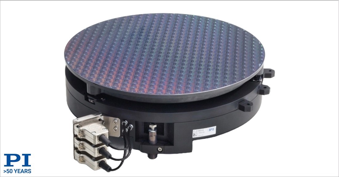
PI’s new nanopositioning technology advancement initiative supports EU-funded project.

Image Credit: PI (Physik Instrumente) LP
Karlsruhe, Germany – 14ACMOS, a new, EU-funded development project for the next semiconductor technology node, is expected to enable the production of chip structures with dimensions down to 14 angstroms (1.4 nanometers). Physik Instrumente (PI) is participating in the research program by developing ultra-high precision nanopositioning systems with accuracies better than one millionth of a millimeter.
High-end microchips manufactured using 3 nanometer technology are the current state of the art. Production technologies for the 2nm technology node are expected to be available as early as next year and for 1.4 nm, i.e., 14 angstroms, by 2027.
The 95-million-euro research project 14ACMOS is co-funded by the European Union and supported by the “Joint Undertaking for Chips” (Chips JU). It brings together the know-how and development expertise of Europe's leading suppliers to the semiconductor industry.The project, which involves twenty-five partners from six countries, is coordinated by ASML, the Dutch world leader in lithography systems for semiconductor manufacturing.
PI has been a system partner to the semiconductor industry for decades and is represented worldwide with nanometer precision motion and positioning systems in a wide range of applications related to semiconductor production. Examples include lithography, metrology, quality control and beam delivery. The nanopositioning systems to be developed as part of the 14ACMOS project must function under vacuum conditions reliably and with very high dynamics to be economically viable.
This project is co-funded by the European Union under grant agreement No 101096772 and is supported by the Chips Joint Undertaking and its members. More information about the 14ACMOS project
The angstrom scale is often used to describe atomic distances. One angstrom is equal to one ten millionth of a millimeter or 0.1 nanometers (nm). For comparison: A human hair is about 80,000 nanometers thick, and diameter of the smallest atom (hydrogen) is about 0.5 angstroms.
Moore’s Law Still Valid
The ongoing miniaturization of semiconductor structures, commonly known as Moore's Law, dictates that the number of electronic circuits doubles approximately every 18 months. This trend was first forecasted by Gordon Moore, co-founder of Intel, back in 1965.
Higher transistor counts on the next generation chips will provide greater computing power to satisfy the needs of AI applications, self-learning algorithms, and autonomous vehicles.
More information on PI’s nanopositioning and motion control solutions for the semiconductor industry
Industries Served
Semiconductor technology