Wafer Stages for Thin Film Metrology and Glass Substrate Inspection

Configurable, granite-based wafer-stage sub-system, new from PI.
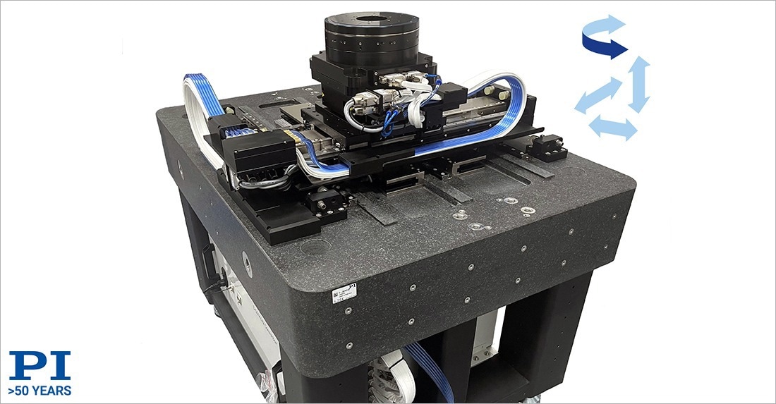
Image Credit: PI (Physik Instrumente) LP

Auburn, MA – PI, a global leader in nanopositioning and motion control, is offering granite-based multi-axis precision motion systems for the automation of wafer metrology, glass substrate inspection and lithography applications. These highly accurate stages are based on modular concepts that allow fast customizations. Several technologies are available including air bearings, rails-on-granite, and several types of piezo drive systems. Large travel ranges of one meter and more can be achieved with a variety of different configurations. The XYZ-Theta example stage shown is designed for thin film metrology equipped with direct drive motors, nanometer resolution encoders, and high-performance ACS motion controllers.

More information on precision motion for semiconductor applications

PI’s advanced design expertise and long experience as a supplier to top tier semiconductor manufacturers and leading system integrators enables us to understand and meet the high demands of the industry, including copy exactly and meeting strict cleanroom requirements.

Industries Served
Semiconductors, photonics, optics, automation, metrology

​​​​​​​

Citations

Please use one of the following formats to cite this article in your essay, paper or report:

  • APA

    PI (Physik Instrumente) LP. (2024, May 31). Wafer Stages for Thin Film Metrology and Glass Substrate Inspection. AZoNano. Retrieved on December 10, 2024 from https://www.azonano.com/news.aspx?newsID=40899.

  • MLA

    PI (Physik Instrumente) LP. "Wafer Stages for Thin Film Metrology and Glass Substrate Inspection". AZoNano. 10 December 2024. <https://www.azonano.com/news.aspx?newsID=40899>.

  • Chicago

    PI (Physik Instrumente) LP. "Wafer Stages for Thin Film Metrology and Glass Substrate Inspection". AZoNano. https://www.azonano.com/news.aspx?newsID=40899. (accessed December 10, 2024).

  • Harvard

    PI (Physik Instrumente) LP. 2024. Wafer Stages for Thin Film Metrology and Glass Substrate Inspection. AZoNano, viewed 10 December 2024, https://www.azonano.com/news.aspx?newsID=40899.

Tell Us What You Think

Do you have a review, update or anything you would like to add to this news story?

Leave your feedback
Your comment type
Submit

While we only use edited and approved content for Azthena answers, it may on occasions provide incorrect responses. Please confirm any data provided with the related suppliers or authors. We do not provide medical advice, if you search for medical information you must always consult a medical professional before acting on any information provided.

Your questions, but not your email details will be shared with OpenAI and retained for 30 days in accordance with their privacy principles.

Please do not ask questions that use sensitive or confidential information.

Read the full Terms & Conditions.