EtherCat®-based high performance motion controllers play a key role in precision automation of highly accurate handling and alignment applications, such as those in laser and materials processing, additive manufacturing, 3D-printing, semiconductor manufacturing and optical inspection systems.
Besides providing robustness and reliability, deterministic behavior with reduced latency, high-speed synchronization with external devices, such as cameras and lasers, is required to attain sub-micrometer path accuracy, high dynamics, exact positioning repeatability and throughput. Safety, state-of-the-art connectivity, and ease of operation for integration into industrial network environments are additional requirements.
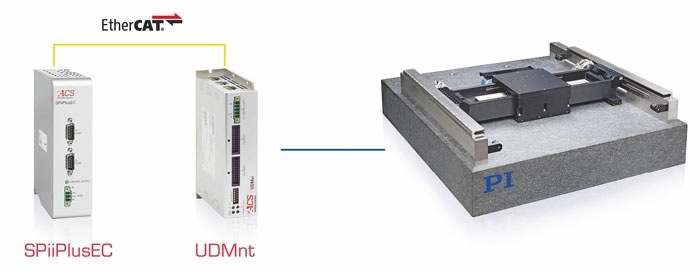
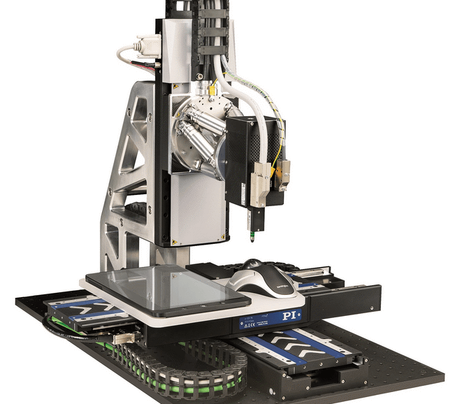
Ether Cat-based modular motion controllers provide the brain power to run multi-axis systems with focus on maximum throughput in industrial nanopositioning applications. (Image: PI / ACS)
The higher the throughput and dynamics targets of a multi-axis precision motion system, the more complete the design method that has to be taken to accomplish success. The best positioning mechanics will not be able to follow multidimensional motion profiles without an industry-grade motion controller that will synchronize the individual axes on a sub-millisecond time scale while simultaneously communicating with a higher-level automation environment. A systems method where control electronics, mechanics and software are engineered by the same team, offers clear advantages for the user.
Customized Complete Systems from One Single Source
When ACS Motion Control united with the PI Group, this was one of the goals. Based on more than 30 years of design expertise in industrial precision automation, the newest generation of modular controllers from ACS now provides the motion control brain power for PI’s engineered motion systems for industrial applications with maximum demands on precision and dynamics. Over the last 40 years, PI’s precision positioning systems have empowered innumerable high-end applications in industries from biotechnology to semiconductor manufacturing.
EtherCat-based controllers make it possible to easily combine different motion subsystems, such as parallel kinematic hexapods and traditional serial kinematics consisting of individual linear and rotary stages. (Image: PI)
Multi-Axis Stage: 6-Axis Hexapod + XY Stage Range Extender for Multi-Axis Motion and Automation
Watch Video: Hexapod with XY Range Extender
100,000:1 Dynamic Range, EtherCAT, Extensive Trigger Functionality
ACS motion controllers are modular by design, scalable, interchangeable and communicate with a variety of Ethernet protocols. They are also EtherCAT masters, responsible for handling all the network nodes (sensors, drives, I/Os) of the EtherCAT network. The servo loop is managed inside each universal drive module for each axis. All current, position loops and velocity work at 20 kHz irrespective of the numbers of axes, a precondition for accomplishing high dynamics with exceptional axis synchronization. Extensive, modular trigger functionality aids incorporation of external devices, such as cameras and lasers.
Performance of V-551 linear motor positioning stage, controlled by with ACS motion controller. The combination of low noise drive technology and proprietary high resolution linear encoders allows for high signal to noise ratio even for step sizes as small as 1nm as shown in the graph above (Image: PI/ACS)
Together with the linear and rotational axes, parallel kinematic or hexapods planar scanners, the controllers are part of a customer-selectable complete system built by PI.
Advanced algorithms in the motion controller reduce jitter, decrease settle times and prevent vibration. Patented technology allows for the design of compact, quiet, PWM drives with dynamic ranges of 100,000:1 – which results in sub-nanometer level standstill jitter and pushes the limits for metrology applications.
Measurements have also revealed these drives to realize nanometer level of tracking errors while scanning a wafer. Additional features are the integrated 3-DOF compensation of positioning errors and yaw compensation for gantry solutions.
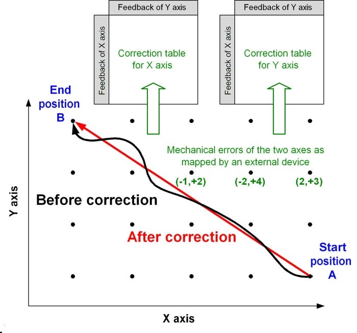
Dynamic error correction improves XY positioning accuracy (Image: ACS)
Tuning and optimization are simplified by a Servo-Boost™ algorithm that detects the root cause of disturbances in real time, and reduces its effect making the system more robust and less sensitive to altering loads and interactions between different axes mounted on the same frame.
The result is enhanced stability and robust control with high positioning accuracy and decreased settling times.
Air-Bearing Planar Stage for Scanning and Wafer Inspection
An example for the application of high-end motion controllers is illustrated in the three-motor planar XY-Yaw air-bearing stage that was produced for wafer inspection. Over the whole travel range of 500 x 1000 mm, it functions with a straightness/flatness of ±10 nm per 10 mm travel. To attain ideal orthogonality alignment between the X and Y axes, the system is mapped on a laser interferometer, and the data is uploaded onto the controller which differs the yaw precisely and dynamically during motion to offer the maximum XY accuracy. The controller also dampens oscillation actively with the profile-shaping algorithm.
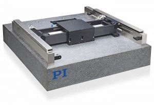
PIglide HS, standard planar air-bearing XY-Yaw linear motor stage for high-precision scanning and inspection applications. (Image: PI)
Air Bearings How do they work? Example XY Air Bearing Stage, PIglide XY-Table
Watch Video: How Air Bearings Work
The air-bearing planar stage is powered by electromagnetic linear motor direct drives. Its modular design enables varied travel ranges and encoder types, based on the required positioning accuracy. The friction and wear-free air bearings ensure constant velocity, extremely level motion and practically unlimited lifetime.
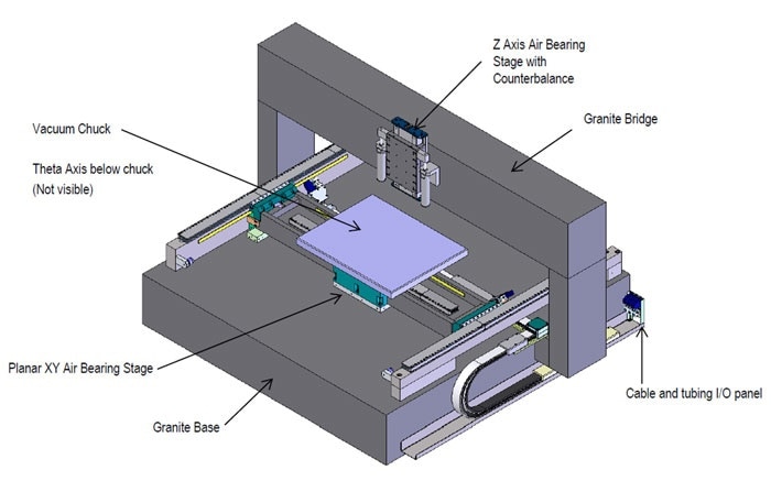
Custom XYZ-Theta-Z air bearing multi-axis system for wafer inspection. The gantry-mounted Z-stage is equipped with a pneumatic counterbalance. (Image: PI)
Highly Accurate Positioning System for Laser Processing
Precision motion control is also needed for laser and imaging processing applications. In the case of laser cutting for instance, a highly dynamic XY positioning system, based on ironless linear motors and crossed–roller bearings is used. Mechanical bearings cannot offer quite the precision of air bearings, but high-end cross roller bearings are good enough for a number of sub-micron-positioning applications and they are more compact than air bearings allowing easy integration into tighter spaces. The compact XY-stage in the example offers a flatness/straightness of ±3 µm over the whole travel range of 200 mm, with load capacity of up to 20 kg and position repeatability of 0.2 µm. The controller used in this motion system supports both position and velocity dependent laser activating to enhance synchronization of motion and laser pulses when cutting arcs or corners.
Integrated low-profile XY linear motor stage system with cross-roller bearings for laser cutting applications. (Image: PI)
The roundness of the points and the gap spacing determine the quality of the cutting line. A special algorithm in the controller helps to synchronize the motion with the laser pulses so that the size of the points and the gaps stay constant even in corners. The laser performance stays constant and velocity of the motion is modified correspondingly. The same applies to cutting circles and arcs. This also avoids inaccuracies that result from a possible discontinuation behavior when moving along an arc. Thus roundness and arc cutting no longer depend on motion parameters.
Similar increases in accuracy can also be accomplished in other application fields. Advanced motion algorithms allow for important throughput increases in industrial multi-axis motion applications by planning ahead and setting motion parameters correctly according to the upcoming segments. The software enables the user to pick whether a corner should be passed with decreased velocity for maximum accuracy, or without velocity alteration so as to improve throughput.
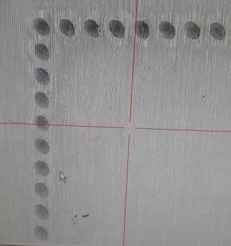
The excellent synchronization between motion and the laser pulse results in a consistent center line distance between adjacent dots (Image: ACS)
The large bandwidth of nano and micro positioning mechanisms and motion controllers along with the systems design experience gained over years between engineering teams at PI and ACS provides an exceptional basis for advanced motion projects in industries from semiconductor manufacturing to medical engineering and nanotechnology.
High End Motion Control for Industrial Precision Multi-Axis Automation Systems
Watch Video: A 10-axis precision automation system (Image: PI)

This information has been sourced, reviewed and adapted from materials provided by Physik Instrumente (PI) GmbH & Co KG - Worldwide.
For more information on this source, please visit Physik Instrumente (PI) GmbH & Co KG - Worldwide.