To use electron or ion beams to create nano-patterns the three methods that are typically used include ion beam milling, beam induced chemistry (deposition and etch), and beam induced lithography. Beam induced lithography is most commonly used for creating useful templates for the manufacture of a range of devices.
This application note provides instructions for writing, preparing, and developing patterns in hydrogen silsesquioxane (HSQ) films. This is a broadly used negative tone electron beam photoresist. These patterning procedures can be easily performed in a well-equipped laboratory even where then there are no detailed lithography tools available. The procedure described is used in a helium ion microscope (HIM). The development and documentation of the steps given below have been provided by Donny Winston of the NanoStructures Laboratory at the Massachusetts Institute of Technology.
Materials and Equipment
To prepare a sample of HSQ on silicon, the materials required are listed below:
- A silicon wafer. The procedure developed in this experiment was with wafers having the following specifications:
- 3" (75mm) diameter
- 356-406 μm thickness
- 1-100 Ω-cm resistivity
- <100> orientation
- Either new or reclaimed wafers can be utilized
- HSQ in MIBK solvent. One such product is XR-1541-006 (Dow Corning).
- Additional MIBK if dilution is desired. A more dilute HSQ solution will result in a thinner film (e.g. Dow MIBK semiconductor grade rinse solvent, Dow Corning).
- Laboratory refrigerator
- Fume hood
- Spin coater
- Ellipsometer
- Standard chemistry lab-ware and solvents, as mentioned below
- Additional equipment may be needed if wafer reclamation is part of the procedure.
Sample Preparation
To prepare the resist coated wafer for lithography, the three steps to be followed are detailed below:
Preparation of Dilute HSQ
As per this procedure, 10 mL of a 10:1 dilution of a 6 %-solids HSQ solution is prepared. The resulting dilution will allow film thicknesses as low as 12 nm. All chemical work must be done in a fume hood to avoid inhalation and spill hazards associated with solvents such as MIBK.
- Remove HSQ from the refrigerator.
- Get MIBK for dilution.
- Gather together a plastic graduated cylinder such as a 10 mL Nalgene CAT NO. 3663-0010, a plastic funnel for pouring HSQ solution and MIBK into the graduated cylinder, a plastic bottle to store the dilution such as a 30 mL Nalgene LDPE bottle with dropper cap, and a solvent waste bottle with funnel6.
- The graduated cylinder and the funnel has to be cleaned with acetone, then methanol, then isopropyl alcohol (IPA), and then dry it with a nitrogen gun. Acetone is an aggressive solvent of organics. Methanol is soluble in acetone, and IPA is soluble in methanol. IPA evaporates rapidly and cleanly. In case the cylinder and funnel have been cleaned previously, an IPA rinse followed by nitrogen-gun drying is sufficient.
- The bottle has to be cleaned through successive rinsing that includes vigorous shaking of the sealed bottle with acetone, methanol, and IPA. Finally, rinse with MIBK.
- Measure out 1 mL of the HSQ solution and then pour it in the bottle.
- Measure 9 mL of the MIBK and then pour it in the bottle. Again, spills can be mitigated by using a fab wipe as a bib for the bottle.
- Swirl the bottle gently for 1 min to mix the 0.6 % solids solution.
- Rinse the funnel and graduated cylinder with IPA.
- Place the manufacturer's HSQ solution into the refrigerator.
- Place the sample in the refrigerator until 10 min before you plan to use it. The solution has to be kept at room temperature before spinning.
Preparation of Clean Silicon Wafers
For the lithography step, a reclaimed or new wafer can be used. To clean reclaimed silicon wafers, the "RCA cleaning: SC1 + SC2" process is recommended.
In case a clean wafer has been stored in fluoroware for more than a few hours or if surface contamination is suspected, such contaminations can be removed by oxygen plasma etching, commonly referred to as "ashing".
It is desirable to re-clean chips rather than a whole wafer, a carrier wafer may be required to support the chips in the asher, subject to the design of the asher. A microwave asher operating at 2.45 GHz has been used previously. An asher using RF power can also work perfectly. The ashing parameters are oxygen flow at 500 mL/min, 1000 W power for 5 min.
If there is no requirement for an area larger than about 1 ~ 1 mm for the lithography, it is recommended to cleave the wafer into 1 ~ 1 cm chips. This cleaving can be done manually using a diamond scribe, but the user should blow the surface dry with a nitrogen gun to remove remaining silicon particles from the surface.
Spinning HSQ on Silicon
- The silicon chip is mounted on the spin chuck. A 100CB spin coater from Brewer Sciences has been used. The equipment is shown in Figure 1.
- The angular acceleration is selected. A value of 10 krpm/sec will ensure an increase to the final angular velocity within 1 sec. High angular acceleration results in thinner films.
- Choose the angular velocity or spin speed and total duration of the spinner. To give a point of reference, spinning at 6 krpm for 31 sec, using a 10 krpm/sec initial ramp, and using a 0.6 % HSQ solution as specified in the above procedure on a ~1 cm2 Si chip, results in a 12-nm film thickness.
- After air-drying, measure the film thickness. One possible tool for this is a Woollam M-2000 H Spectroscopic Ellipsometer (λ= 240-1000 nm), operated at 70‹ incidence. This equipment is shown in Figure 2.

Figure 1. CEE100 Spin Coater.
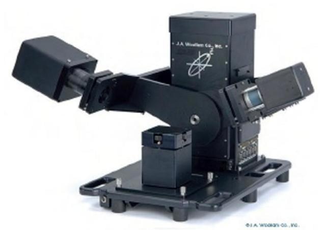
Figure 2. Spectral Ellipsometer.
Exposure in the ORION PLUS
Guidelines for setting up a lithographic exposure in the HIM are provided below. These guidelines can be applied to any lithography task.
- Make sure that there is a target for beam focusing and stigmation near the exposure area. For example, a diamond scribe can be utilized to put a scratch mark near one corner of the chip.
- The sample is loaded and navigated to an area of the focusing target adjacent to the desired exposure area. This could be the end of a scribe scratch very near the center of the chip. Focus and stigmate.
- While using an external pattern generator, switch to external control from within the ORION PLUS user interface (UI) as shown in Figures 3 and 4. Check the voltage polarity on blanker activation for the pattern generator to decide whether to select blanker active high or blanker active low in the ORION PLUS UI.
- Based on the pattern generator, there may also be additional parameters to set. With the Nabity NPGS, for example, one must set a "mag scale" parameter equal to the ORION PLUS magnification ~ field of view (in μm). For example, if the field of view at 1000 X is 127 μm, the NPGS mag scale is 127000. Also, while using the maximum dynamic range of beam deflection in NGPS, i.e. } 10 V, it is essential to set the ORION PLUS field of view to be double that expected by the pattern file in NPGS. Otherwise, the pattern will be written at 50 % scale. The calibration value also varies based on the type of deflection amplifiers in the HIM.
- The first pattern must include a dose array. The critical dose for exposure can vary with HSQ dilution and spin thickness. An example areal dose is 30 μC / cm2. An example line dose is 0.25 nC / cm. An example point dose is 0.25 fC.
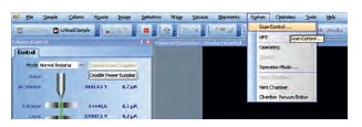
Figure 3. Scan Control command, under the System menu in the ORION PLUS UI.
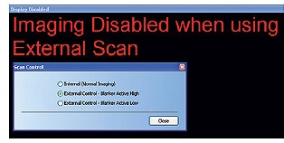
Figure 4. Scan control pop-up and user notification.
Preparation of "Salty" Developer
Using this procedure, a 500 mL aqueous solution of 1 wt % NaOH and 4 wt % NaCl is obtained. This solution is a high contrast developer for HSQ. The recipe requires de-ionized (DI) water, NaOH pellets, granular NaCl in the form of table salt and a milligram scale.
- Rinse a 1 L plastic bottle with isopropyl alcohol (IPA) and then DI water.
- Pour in 500 mL (500 g) DI water.
- Measure and pour in 5 g of the NaOH pellets. NaOH is a high-concentration base and needs to be handled with care.
- Measure out and pour in 20 g NaCl. Stir the mixture till total dissolution is achieved.
Development
To develop a small (~1~1 cm2) sample, only a small developer volume is needed. This is a simple and straightforward procedure, taking just a few minutes.
- Nearly fill a 10 mL Pyrex beaker with salty developer.
- Dip and hold the sample with tweezers in the developer for 4 min. Swirl gently.
- Rinse for approximately 30 sec in running DI water.
- Rinse for approximately 30 sec with isopropyl alcohol.
- Dry with a nitrogen gun.
Inspection of Results
Inspection must be performed in SEM. This provides a good contrast between the silicon and HSQ material. Imaging the sample in the HIM can modify the tiniest features, so metrology of patterning results using HIM must be done carefully.
Figure 5 shows representative results for a pillar array patterned into 30 nm of HSQ. Fig. 5(a) shows an underexposed array, where only a portion of the developed pillars remain standing. Figure (b) shows a properly exposed array, and Figure (c) shows an overexposed array, where the feature size has grown.
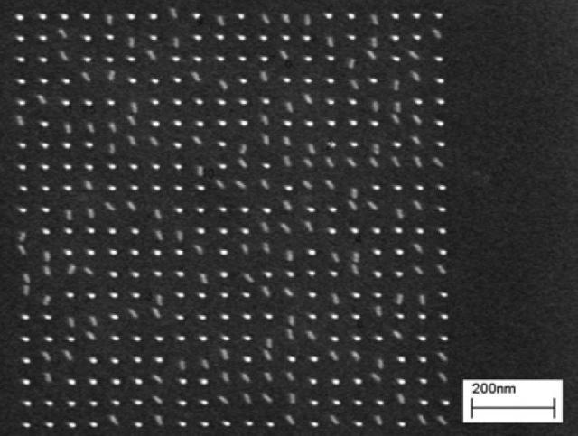
Figure 5(a). Pillar array exposed at 0.25 fC per pillar.
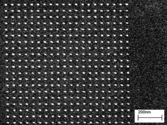
Figure 5(b). Pillar array exposed at 0.42 fC per pillar.
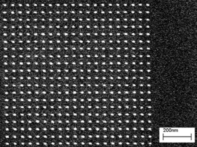
Figure 5(c). Pillar array exposed at 0.70 fC per pillar.
An illustrative comparison of this lithography result to EBL. Figure 6 shows a pillar array created by 10 keV EBL9.
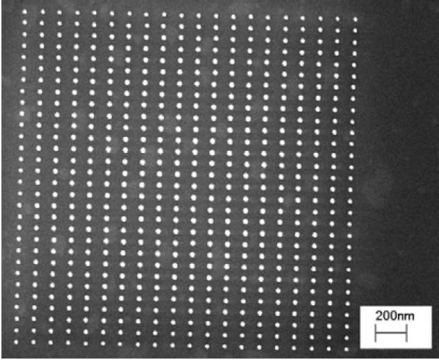
Figure 6. Electron Beam produced pillar array exposed at 24.88 fC per pillar.
While these pillars were created in a thicker (70 nm) HSQ layer, there are differences to highlight. First, the minimum dose to expose the entire array is 25 times higher for EBL normalized for the height difference. Most significantly, there is a strong dependence of pillar size on position within the array. Pillars nearer the edge of the array are narrower. This takes place due to the EBL proximity effect, where beam writing in one spot imparts a dose on neighboring areas. The histogram in Figure 7 shows the tighter distribution in size of the HIM created pillars.
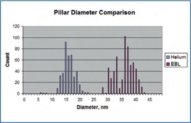
Figure 7. Histograms of pillar size distributions in HIM and EBL

This information has been sourced, reviewed and adapted from materials provided by Carl Zeiss.
For more information on this source, please visit Carl Zeiss.