Electron beam lithography (EBL) is an important technique, which is used to design devices, systems and functional materials at the nano scale. In this miniaturization technique, large-scale products are converted into small-scale structures. Principally, the fabrication procedure can be performed in a traditional scanning electron microscope (SEM) integrated with an extra control unit. During the EBL process, both SEM and light microscope (LM) are utilized for control and investigation of the developed nanostructures at the same sample areas. At this stage, the "Shuttle & Find" interface for correlative microscopy provides a suitable solution for exact relocation of regions of interest for this application.
EBL Process
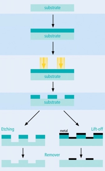
Figure 1. Electron beam lithography process. (Insert the flowchart given in page 2. but don’t include the content given on the right side)
The above figure shows the series of nanostructuring during the EBL procedure. The exposure of a sensitive resist with an electron beam is the core of the EBL process. The resist is often a polymer dissolved in a liquid solvent, which is coated onto a surface and baked to form an even thin layer. During electron beam exposure, the solubility of the resist is altered, causing a dissolution variation with areas that are non-exposed. Following this, the pattern is developed using a liquid developer. Lastly, the combination with processes, like dry or wet etching, lift-off of evaporated material, and/or electro- deposition completes the fabrication of structure.
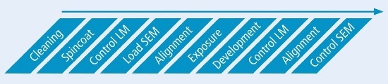
Figure 2. Workflow during EBL nanofabrication.
The flowchart given above displays the complete workflow of a traditional EBL process. LM and SEM are utilized a number of times for exposure or control. Owing to the nature of resists, the stage navigation in the SEM should be carried out with the beam blanked so as to prevent exposure. For such exposures, "Shuttle & Find" offers a suitable solution and prevents extensive stage alignments.
Instrument
An EBL instrument includes a vacuum system, an electron gun, and a computer interface for beam control and pattern creation. A standard SEM can be configured by simply adding a hardware controller. This can be done easily and does not require much SEM modification. The present task can be done on ZEISS SUPRA 40 Field Emission SEM integrated with a Raith Elphy+ hardware controller and an Axio Imager.Mlm light microscope with motorized stage.
Application Process
The "Shuttle & Find" software module based on AxioVision needs to be placed on SEM and LM. Following the preparation of sample with EBL resist, it is fitted onto the correlative sample holder, which in turn is calibrated in the light microscope by utilizing the Shuttle & Find automatic calibration process. A coordinate system on the holder relating to the LM stage coordinates is defined in this step. Then, a clean and even area is selected in the LM for later exposure. It is necessary to perform exposure at the appropriate place, where resist is even and lacks dust particles. Hence, a region of interest is selected in the upper right corner as shown in the figure below. The Shuttle & Find software saves the regions of interest.
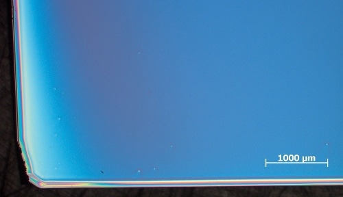
Figure 3. Corner of a sample prepared with EBL resist for control in LM.
In order to perform exposure, the sample holder as well as the data on the regions of interest is shifted to the SEM. After doing the same calibration process as performed in LM, the selected regions of interest are relocated in the SEM and magnification is altered. Following fine calibration, the relocation precision becomes less than 10 µm. After developing the resist, the sample is again shifted to LM for the next step. Since the "Shuttle & Find" interface enables relocation both in SEM and LM, it is employed for relocation of the writing field so as to eliminate lengthy searches.
Another illustration of LM control after EBL exposure is shown in figure 4. Once the right EBL parameters are established by the test structure, the Diffractive Optical Element’s structure is exposed into a writing field. After this, the sample is shifted to the LM and then the writing field is relocated accurately for control.
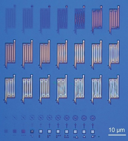
Figure 4. LM control image of EBL dose test structure.
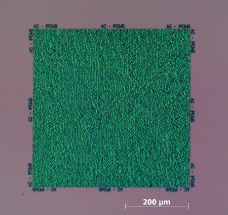
Figure 5. LM image of a Diffractive Optical Element exposed by EBL.
Conclusion
The "Shuttle & Find" interface allows enhanced productivity in EBL nanofabrication as a result of quick accurate and reliable workflow. The workflow is scaled up considerably as the means of searching the same regions of interest in both microscopy modes has now been automated. "Shuttle & Find" can be used with CrossBeam workstations, and hence the sample can be relocated there for additional nanofabrication. Moreover, specific nanostructures can be adjusted by Focused Ion Beam milling.

This information has been sourced, reviewed and adapted from materials provided by Carl Zeiss.
For more information on this source, please visit Carl Zeiss.