When it comes to the fiber optic data highway, silicon photonics (SiP) sets the pace. Data rates in the TBit/s range can benefit rapid Internet access, cloud computing, big data, server farms, and an extensive range of other computer-supported services requiring high transmission speeds.
Despite these advances, there are several issues that need to be resolved for the development and testing of advanced silicon photonics wafers. It is important for automated solutions to function consistently even under adverse industrial conditions and operate continuously with a high level of precision. In addition to this, separate solutions are also needed, because the wafer can place different kinds of demands on the production and testing equipment.
Normal and easily scalable processes, which are optimized for large-scale manufacture of semiconductor components, are used by SiP. With SiP, optical transceivers, and electronic logic circuits, like those utilized for computing, are incorporated within the same wafer. The low-power microchips that are obtained subsequently relay the data at bandwidths in the Tbit/s range and with a low generation of heat. However, given the fact that the value of a packaged SiP circuit considerably increases, compared to the raw circuit on a wafer, it is essential to perform wafer-level testing of individual circuits prior to dicing and packaging.
It is also important to test optical outputs and inputs. This method requires accuracy that is several orders of magnitude higher than can be achieved with conventional electrical wafer probing equipment. It should be ensured that both outputs and inputs are accurately aligned to the optical fibers joined to the test system. That is a major issue, because in silicon wafers, optical waveguides will typically have a core diameter of just 150 to 200 nm, so to prevent losses, it must be ensured that alignment equipment has a minimum of 10x higher resolution. As a result, it is not easy to control this type of automation task because the highest accuracy during adjusting, positioning, and handling is equally important as the highest speed possible for fulfilling the requirements of industrial production.
Precision Fiber Alignment: Multi-Channel Fiber Adjustment in Real Time
PI (Physik Instrumente) from Karlsruhe is a solution supplier for precision positioning systems and drive technology. The company studied this matter at a closer level and eventually designed a new system that enables rapid fiber alignment, allowing alignment, testing, and optimization of the light output and input at the individual output and input coupling point within a second (Figure 1).
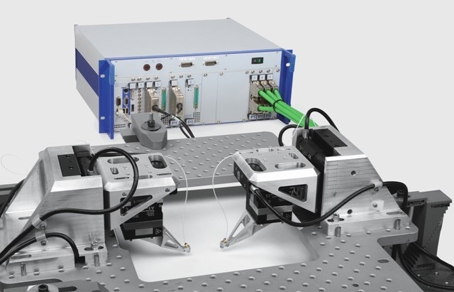
Figure 1. Industry-suited complete systems for wafer probing in silicon photonics.
With the aid of this complete system, rapid data throughput rates are ensured during industrial production. The system includes two compact, similar-looking positioning units with a small footprint of just 100 × 100 mm, so they do not take up much installation space.
The application-specific controller is the core of the system and comes with many integrated tracking and alignment algorithms needed for optical alignment, which reduces the load on the higher level control. Communication between the host computer and the controller occurs through an RS-232 interface, USB 2.0, or Ethernet. The system is supplied with a high-performance software package, enabling users to develop applications under OS/X, , Linux, and Windows in a rapid way.
Coarse and Fine Adjustment
Positioning is carried out in two phases: powered by closed-loop DC motors, a three-axis positioning stage manages the first task of coarse adjustment and moves to the relevant coupling point over travel ranges of several tens of millimeters, with up to 50 nm precision. Fine positioning of the fibers is carried out with an extra three-axis positioning unit.
Powered by piezo actuators, the system attains 1 nm resolutions, with travel ranges of 100 × 100 × 100 µm and response times in the microsecond range. Through FEA-optimized flexure joints, the high-performance piezo actuators are incorporated into guiding systems and do not contain backlash and friction. Since sensors, guides, and actuators are capable of working without wear, the systems are highly durable and reliable, and are ideal for meeting industrial needs in multiple-shift operation on a continuous basis.
More Degrees of Freedom
During wafer packaging or probing, one or more issues can occur based on the application: for instance, if the fibers have to be positioned at varied angles or if there is a need to offset the tilt angular errors, then more axes would be needed. It is possible to achieve serial stacking of more axes on the positioning stage; however, the restrictions offset the benefits of this method. In this case, the precision would be compromised, since more guiding errors will bring down the overall accuracy.
As a substitute, a more suitable solution would be to integrate the fine positioner with a hexapod parallel-kinematic positioning system. This is because, when compared to serial kinematics, all actuators integrated into parallel-kinematic systems directly act on the same platform and guiding errors cannot build up (the case with stacked systems) considerably increasing the precision.
Featuring six-axis parallel kinematics, hexapods provide additional benefits for fiber alignment. As these have low moving mass, they offer relatively higher dynamics (Figure 2).
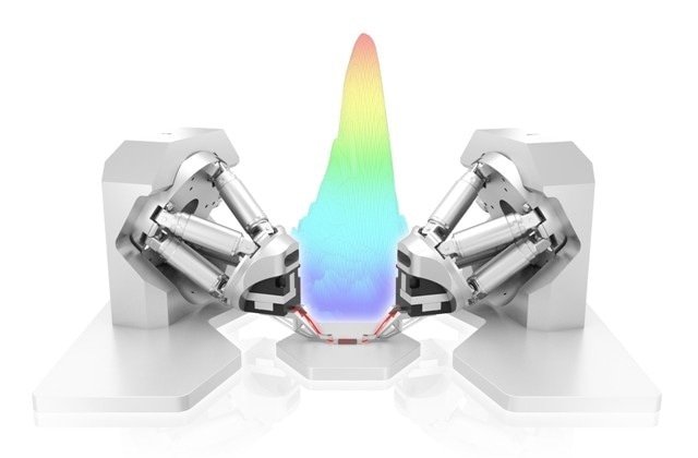
Figure 2. Wafer level alignment with a two-side 6-axis Hexapod and a piezo scanning stage for fine alignment.
Another aspect is the random center of pivot point or rotation that can be programmed through a single command. For instance, the H-811 Hexapod (Figure 3) provides rotational travel up to 42° and travel linear ranges up to 34 mm. The fine positioned based on piezo actuator combines with the hexapod platform.
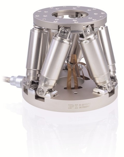
Figure 3. This parallel-kinematic six-axis positioning system is also ideal for fiber alignment.
Other parallel-kinematic positioning systems are available for different load requirements and travel ranges, and these can be integrated with the fine positioned (least incremental motion of 0.1µm /2 µrad and velocities of 10 µm/s to 10 mm/s). The planar parallel positioning system is built on three XY stages driving a single platform via three permanent struts. This design not only enables more flexibility, but also promotes extended travel ranges on the XY plane.
High-Performance Software
All algorithms required for fiber optic alignment are already incorporated in the digital controller, regardless of which positioning system is suitable for the application. Further, PI’s digital motion controllers come with a comprehensive software package (Figure 4), which spans all application features, from simple start-up to effortless control of the system through the graphical interface, and quick and transparent incorporation within external programs.
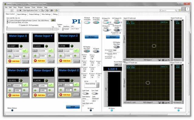
Figure 4. An example of real-time system control
Through a virtual controller, application programs can be developed without the need to have all of the components. For instance, simulation tools help to measure the workspace, or alternatively objects can be incorporated to prevent collisions.
A mobile app allows wireless control and monitoring; example applications and development libraries simplify implementation; and several software environments and common programming languages are supported, such as C, C++, Visual C++, Python, Visual Basic and LabVIEW or Delphi, TANGO, MATLAB, EPICS, µManager, in addition to all programming environments that support DLLs loading. This ultimately helps in achieving customized industrial applications with respect to probing and packaging of the wafer in silicon photonics.

This information has been sourced, reviewed and adapted from materials provided by Physik Instrumente (PI) GmbH & Co KG - Worldwide.
For more information on this source, please visit Physik Instrumente (PI) GmbH & Co KG - Worldwide.