Engineered surfaces and thin films are utilized in a range of applications such as precision optics, data storage, and semiconductor electronics. In the majority of applications, surface roughness and the corresponding texture of these device components directly affect their total performance and quality.
The quantification of morphology and surface roughness can be crucial to formulate a quality control metric for the end product or to verify a distinct processing step.
The selection of an instrument that is most compatible with surface roughness measurements heavily relies on the particular material to be measured along with the predicted shape and size of its surface features.
It is becoming more critical to characterize surface roughness at the scale of nanometers or less as device dimensions in a range of industries continue to grow more compact.
The equipment frequently employed for this use are atomic force microscopes (AFMs), scanning electron microscopes, and interferometric optical profilometers.
The AFM is the only method among these that provides the ability to quantify the majority of material types (Table 1) and unrivaled three-dimensional spatial resolution. The AFM offers total 3D surface measurement by imaging topography (height), as demonstrated in Figure 1.
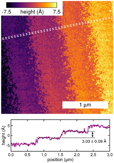
Figure 1. Topography image of a silicon carbide wafer [6H SiC (0001)]. The graph shows the average profile between the white lines in the image and gives a step height of 3.03 ± 0.08 Å between adjacent terraces.
Table 1. Comparison of tools for surface characterization. Specifications given for non-AFM tools are typical ranges for commercial instruments. Additional detailed comparisons can be found in Ref. 1. *Both AFMs and scanning electron microscopes can provide information about materials properties beyond topography. For example, AFMs can measure a host of electrical (e.g., conductivity, permittivity), mechanical (e.g., elastic modulus), and functional properties (e.g., piezoelectric response). For more information, see Ref. 2.
| |
Oxford Instruments Jupiter XR AFM |
Scanning Electron Microscopes |
Interferometric Optical Profilometers |
Stylus Profilometers |
Relevance |
| Lateral resolution |
<1-20 nm |
<1-20 nm |
200-500 nm |
1000-10,000 nm |
Accurate nanoscale surface roughness measurements require nanometer-scale resolution. |
| Height resolution |
<0.025 nm |
No true 3D measurements possible |
1-10 nm |
0.5 nm |
| Measurement type |
Surface topography (3D) and surface properties* |
Surface morphology (quasi-3D) and composition* |
Surface topography |
Line profiles (inefficient for surface mapping) |
Areal surface roughness measurements require accurate imaging of 3D topography. |
| Measurement time (per site) |
<1 minute |
<10 seconds |
<10 seconds |
<1 minute |
Throughput of multisite measurements is affected by time spent per site. |
| Surface material limitations |
Any material type can be measured up 200 mm in diameter and 35 mm in height |
Must be conductive (or coated) and vacuum compatible |
Large variations in reflectivity and refractive index, steep slopes or edges, and very thin films can be problematic. |
Most materials can be measured unless very soft and/or sticky |
Many inspection tools have constraints on the types of materials that |
AFM topography images provide information on the complete surface morphology, can determine nucleation and growth modes, differentiate between amorphous and crystalline phases, and can highlight defects.
Images can be investigated to determine areal surface roughness parameters for example statistics on the domain and grain size or Sq (root mean square roughness) and Sa (3D roughness average).
Distinct line sections can be employed to establish film thickness, step heights, and even lattice spacings. While AFMs offer a range of benefits, it is crucial to note that not all AFMs provide the same ease of use, performance, and capability.
For example, certain models provide exceptionally high performance but can only hold a single, small sample (normally 1 to 2 cm) at once. Jupiter XR is a high-performance AFM that can handle a series of smaller samples and larger samples, for example, 200 mm wafers.
Commercial AFMs are quickly developing, so the latest models can be very different from those released just a few years ago. For example, certain AFMs still employ old-fashioned piezo tube scanner technology.
These scanner configurations are restricted to a significantly slower image acquisition time (5 to 10 minutes for each site or longer), are vulnerable to a greater number of imaging artifacts, and have very fragile, easy-to-break components that make them much less reliable and hard-wearing.
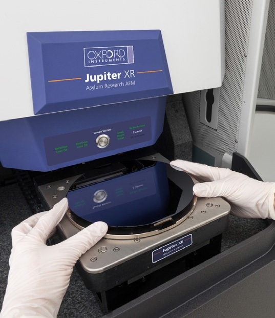
Figure 2. The Asylum Research Jupiter XR AFM holds samples as large as 210 mm, such as this 8-in wafer.
The Jupiter™ XR Large-Sample AFM: High-Speed AFM with Top Performance for Surface Roughness Measurements
The Asylum Research Jupiter XR AFM (Figure 2) has recently been introduced by Oxford Instruments.
Asylum’s expertise in producing high-performance AFMs has been leveraged by Jupiter to offer a completely new AFM with a large inspectable area. It acquires high-resolution images, along with dependable sub-nanometer roughness measurements, high measurement confidence, and high throughput.
These benefits are outlined in further detail and portrayed in the case studies shown in Figures 3 to 6.
Jupiter XR AFM provides a fully addressable, 8-inch inspectable sample stage in its regular configuration. Jupiter can handle large samples of up to 35 mm in thickness and 210 mm in diameter.
The other option is where several smaller samples (such as those placed on ~10 mm sample disks) can be magnetically fixed on the sample stage for sequential evaluation.
The fully addressable motorized sample stage enables the acquisition of images anywhere in a 200x200 mm2 range with no requirement for samples to be rotated. The full wafer accessibility allows efficient inspection of wafers leading to higher productivity and throughput.
Case Study #1: Surface Characterization of Glossy Paper Coating Process
The surface roughness, formulation, and morphology of paper coatings directly affect the appearance and quality of the print. These features are precisely customized to a range of end uses, inks, and printing techniques.
While large-scale coating uniformity is essential, the coating’s surface roughness at the nanoscale significantly affects how the ink reacts to the paper.
AFM is the preferred equipment for this kind of characterization. Figure 3 provides examples of a consumer-grade, inkjet photo paper imaged with the Jupiter XR AFM. The images show the surface characterization advantages offered by the Jupiter AFM at very dissimilar length scales.
The full scan range 100 μm image demonstrates some scratch marks (shown by arrows) and the waviness of the paper (where the brighter areas are higher and the darker regions are lower).
This type of AFM data offers information regarding the quality of the product and may affect the handling techniques to mitigate the bending and scratching of the paper.
The 5 μm size image adjacent to this offers information about the uniformity of the paper sample’s finer grain structure. It can be employed as a guideline for process optimization in the future.
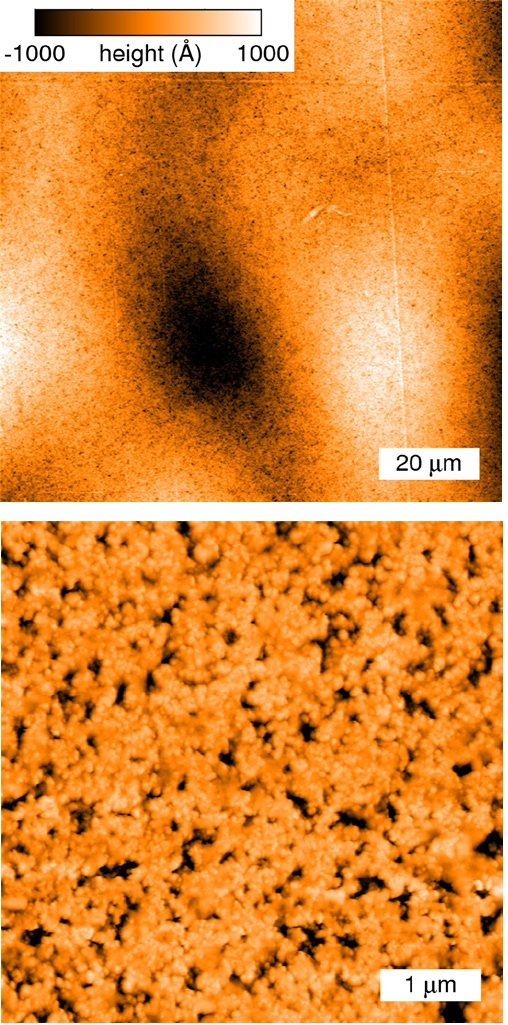
Figure 3. Topography images of glossy printer paper demonstrate that height parameters in addition to Sa can more fully describe surfaces. Skewness (Ssk) is a measure of the distribution of features relative to the mean, where Ssk > 1 indicates a surface dominated by peaks and Ssk < 0 indicates a surface with pits or valleys. Kurtosis (Sku) is sensitive to the sharpness of the peaks and/or pits: Sku > 3 indicates especially sharp features, Sku = 3 indicates a normally distributed surface, and Sku < 3 indicates a more gradually varying surface. (z) Over a very wide scan size (100 μm, 195 nm pixel size), the coating exhibits longer-scale waviness (Ssk=-0.49, Sku=0.58, Sa=235.8 Å). (bottom) However, at a smaller scale (5 μm scan size, 10 nm pixel size), it is evident that the coating also contains much finer grain structure with interspersed pits (Ssk=-1.49, Sku=3.15, Sa=231.1 Å). Though the apparent roughness is very similar at both length scales, the skewness and kurtosis parameters accurately describe the gradual, rolling waviness at longer scales and the pitted surface at smaller scales.
Jupiter XR ultra-low noise floor provides unparalleled sub-nm surface roughness quantification. Asylum’s core of advanced AFM technology has been applied to ensure that Jupiter can quantify surface roughness below the detection range of alternative characterization methods.
Asylum Research AFMs can quantify roughness 2 to 4× lower than the majority of alternative AFMs. The ultra-low noise floor of 0.25 Å means the Jupiter AFM has the minimum resolvable height determined by electronic and mechanical instrument noise. This allows the Jupiter AFM to quantify angstrom-scale surface roughness precisely.
Case study #2 provides an example where differences in processing environments can be observed through small variations in the characteristics of the surface.
Jupiter XR AFM enables increased productivity and high throughput. Jupiter can image 5-20x quicker compared to the majority of AFMs. A single image can routinely be taken in under 2 minutes and as short as 15 seconds (relying on total roughness and scan range).
Its highly efficient motorized sample stage repositions between sites in 5 seconds or under with micrometer accuracy. High-speed positioning and scanning are particularly beneficial when blended with Jupiter’s capability to acquire images automatically, as outlined in case study #2 (see Figure 4).
Case Study #2: Automated Inspection of Epitaxial Silicon Wafer Roughness
Epitaxial layers are widespread in contemporary semiconductor processing. Silicon epitaxy processes produce accurate layers with various dopant concentrations and types, while heteroepitaxial layers of III-V compounds and different materials allow even more choices.
A further advantage of epitaxial layers is their exceptionally low surface roughness in contrast to substrates produced by chemical-mechanical polishing.
Figure 4 provides an example of roughness quantification on a wafer with an epitaxial silicon layer. It shows Jupiter’s capability to perform angstrom level roughness quantification along with automating measurements at various locations on the wafer.
Unique blueDrive™ cantilever excitation creates high reliability and confidence in the measurements. Surface roughness quantification frequently affects essential business decisions, so it is crucial that measurements are reliable, and the equipment is dependable.
The unique blueDrive tapping mode technology from Asylum enhances imaging stability in contrast to traditional AFMs that utilize piezo excitation. This prolongs the lifetime of the tip, which, in turn, allows for repeatability and consistency in the roughness results (see Case study #3, Figure 5).
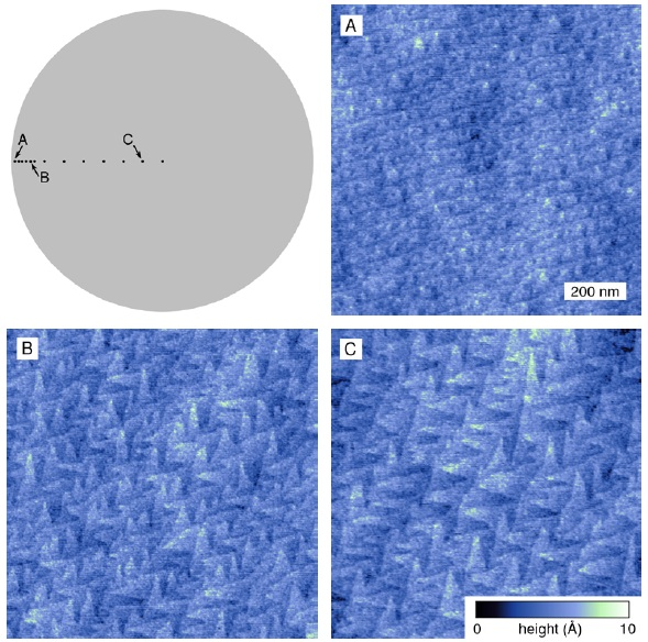
Figure 4. Non-uniform grain size is often observed in epitaxial silicon layers, especially near the wafer edge where greater variations in process conditions may occur. As shown in the diagram, a series of locations on a 150-mm (6-in) wafer was pre-defined in software and used in an automated routine to acquire topography images. (A) Image acquired 200 μm from the wafer edge with Sa=0.785 Å. (B) The image at 1.6 mm from the edge with Sa=0.833 Å. (C) Image acquired 62.4 mm from the edge (12.8 mm from the center) with Sa=0.902 Å.
Case Study #3: Quality Control of Disk Drive Media
Magnetic hard disk drives are still preferred over solid-state drives in areas that demand a considerable amount of affordable data storage.
This benefit has been upheld by the continuous expansion of the data storage density of magnetic disk media. Attaining these high densities has led to a related decrease in media roughness.
The example in Figure 5 demonstrates roughness quantification on the substrate of a contemporary lubricated disk media. Jupiter’s exceptional measurement accuracy, along with its high measurement throughput, are shown by its ability to capture 1000 images while unattended for 15 hours.
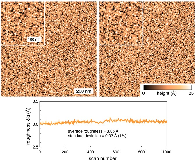
Figure 5. These topography images of a glass disk media substrate are the first and last in a sequence of 1000 acquired over 15 h of unattended operation (~54 seconds per image). In each image, the inset is a digitally zoomed magnification of the lower-left region to help show the finer structure. The graph shows that the measured roughness Sa remains constant within 1% over the entire period, demonstrating the remarkable stability enabled by blueDrive tapping mode imaging.
Case Study #4: Quality Assurance of Chemically Strengthened Display Glass
Modern mobile devices are more adaptable to scratches, bumps, and drops than ever before due to chemically strengthened display glass.
These exclusive formulations of glass undertake an ion exchange process wherein potassium ions replace sodium ions close to the surface. This produces compressive surface stress that makes the glass sheet significantly stronger.
Figure 6 demonstrates measurements on chemically strengthened display glass taken at various length scales. The images show how Jupiter’s adaptable scan range and exceptional resolution allows it to analyze both scratch resistance and overall roughness.
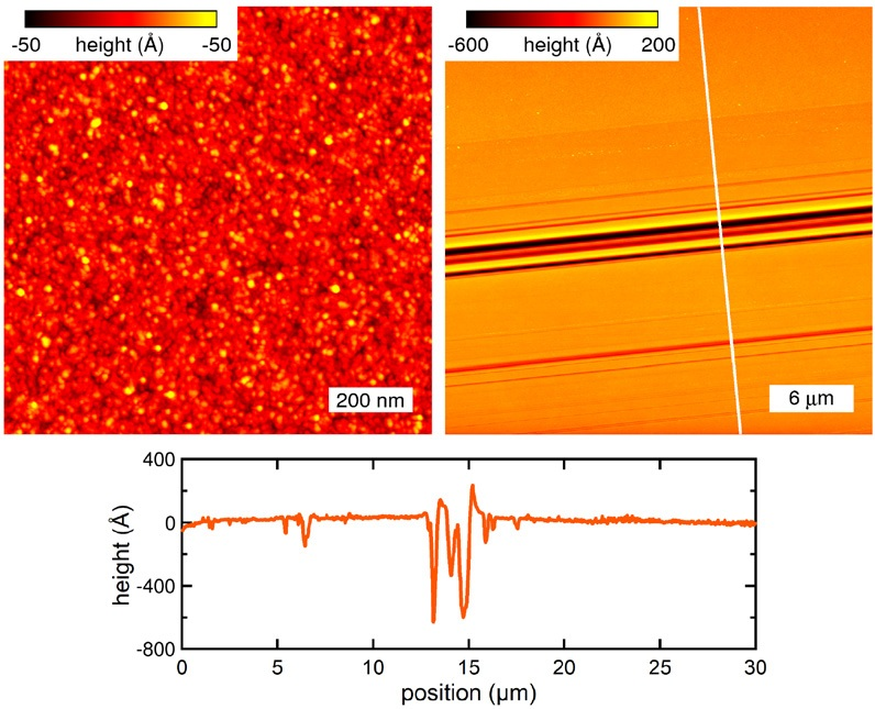
Figure 6. Many applications for display glass demand both low surface roughness and high abrasion resistance. (left) Example of routine roughness measurements made in 52 seconds per site. With a 1 μm scan size, the image gives Sa=9.70 Å. (right) A glass sample was subjected to intentional scratching with metal tweezers, and a large-area image (30 μm scan size) was completed to characterize the dimensions of the scratch. The profile corresponding to the white line in the image shows the damage actually consists of a series of fine parallel scratches. In real QA measurements, such testing could be done using a calibrated load to initiate the scratch (e.g., via a tribometer).
Jupiter XR AFM: The Optimal Tool for Nanometer-scale Surface Roughness Measurement
The Jupiter XR AFM characterizes angstrom and nanometer-scale surface roughness on nearly all materials with ease. When contrasted with regular large-sample AFMs, Jupiter offers greater reliability, more efficient imaging, and a higher resolution.
AFMs can easily quantify much smaller roughness values and a broader range of geometries and material types compared with optical profilometry. Combined with its high measurement accuracy and optimized throughput, Jupiter XR is the instrument of choice for nanoscale surface roughness measurements.
References and Further Reading
- P. J. D. Whiteside, J. A. Chininis, and H. K. Hunt, Coatings 6, 35 (2016).
- For more resources on AFM characterization of thin films, see https://afm.oxinst.com/thin-films

This information has been sourced, reviewed and adapted from materials provided by Asylum Research - An Oxford Instruments Company.
For more information on this source, please visit Asylum Research - An Oxford Instruments Company.