A persistent problem in scanning electron microscopy is the deposition of hydrocarbon contamination induced by an electron beam. Generally, the deposition of contamination on a specimen is a negative and unnecessary effect (although it has been managed and used positively to produce atomic force microscope (AFM) probes).
While the vacuum readings seem to be comparatively good on many occasions, the electron beam still leaves alarming marks of contamination on the specimen.
This implies that in a CD-SEM, repeated measurements cannot be performed without additional and, at times, excessively high measurement errors that result from 'carry-over.'
Carryover essentially means the increased dimension size caused by the deposition of hydrocarbon contamination induced by the electron beam on the boundaries of the structure being measured.
The hydrocarbon moieties that are being deposited come from a broad range of sources, such as the vacuum system, stage lubricants and the sample itself.
During the time required for just a single measurement, the specimen is likely to change and the degree of this change is not known unless an ideal contamination measurement method is identified and routine monitoring is employed.
In a previous report, certain causes of contamination in laboratory scanning electron microscopes (SEMs) were analyzed and possible solutions were demonstrated (Postek, 1996).1 This article builds on that previous study and provides an extra active monitoring and control method to overcome this issue.
Materials and Methods
A Hitachi2 S-4700 laboratory SEM, an S-806 tilt SEM, and Hitachi S6280-H CD-SEM were employed throughout this analysis. The two former instruments were equipped with 150-mm wafer stages, while the CD-SEM was provided with two turbomolecular pumps and two Ebara dry pumps.
The tilt SEM was also equipped with one turbomolecular pump and two rotary pumps.
The S-4700 laboratory SEM was fitted with the factory-installed pumps—one diffusion pump and two rotary mechanical pumps. The specimens used in the analysis were diced chips or clean wafers obtained from wafers designed with different processes employed in silicon integrated circuit technology.
In this analysis, the rate and amount of contamination deposited on these specimens were investigated and some of the potential ways of decreasing the effects of contamination, such as a novel anti-contamination apparatus, called Evactron®, were also analyzed.
Evactron®
The Evactron2 is essentially an automatic plasma cleaning and vacuum monitoring system. It can measure the level of vacuum and, with the help of valves, also regulate the pressure of the gases that are introduced into the chamber required for plasma cleaning.
The system has a built-in power supply to fuel a plasma-generating head. Figure 1 shows the schematic diagram of the Evactron cleaning head.
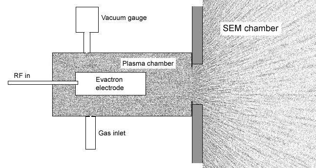
Figure 1. Schematic diagram of the Evactron cleaning head. Image Credit: Evactron (XEI Scientific)
The unit is placed on the wall of the SEM sample chamber and includes a controller that can be configured to automatically regulate the entire cleaning procedure.
The cleaning process is performed at a relatively higher pressure of 40 to 100 Pa when compared to the typical operating pressure of 10−3 to 10−4 Pa of the specimen chamber. To begin the cleaning cycle, the necessary valves are closed to isolate the specimen chamber from the electron optics.
In the ideal case, the specimen chamber can simply be isolated from the molecular or diffusion pump.
In other examples, the process will differ based on the design of the vacuum system. The subsequent step is to allow the gas (filtered, clean, room atmosphere, or oxygen-argon mixture for more rapid cleaning) to enter the specimen chamber and subsequently steady the pressure at its optimal value of 80 Pa.
Once this point is reached, the cleaning head is subjected to a high (13.56 MHz) frequency power for a few minutes. The power applied and the time duration rely on the chamber size. This process provides a gentle plasma cleaning. Within the chamber, the nascent oxygen quickly reacts with the vacuum residues, and the products are pumped out.
To speed up this step, it is advantageous to apply a clean N2 flush. This step is necessary in the case of an oxygen-argon gas mixture. And this process can easily be made fully automatic, which means the user only needs to initiate the unit and wait until it has been completed and the SEM is set for its routine work schedule.
Some commercially available equipment has been identified in this article to sufficiently explain the experimental process.
However, this identification does not indicate endorsement or recommendation by the National Institute of Standards and Technology, and similarly, it does not indicate that the equipment identified is actually the best available tool for the purpose. EVACTRON is a registered trademark of XEI Scientific.
Results
Figure 2 shows the contamination deposition behavior of a pair of CD-SEMs. Each instrument was used to examine the same UV photoresist wafer.
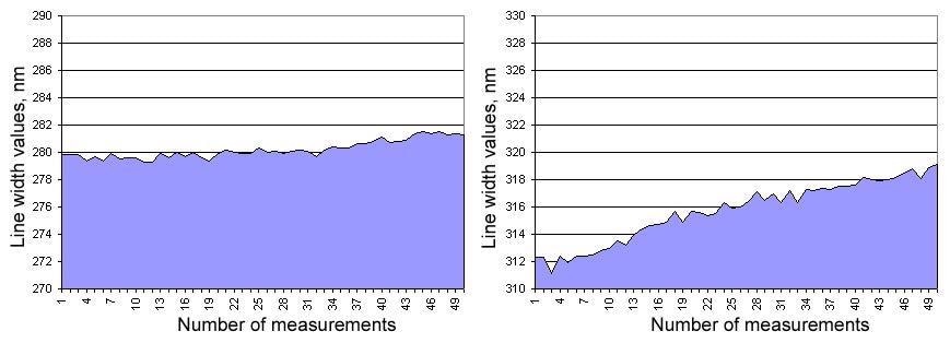
Figure 2. The results of 50 repeated line width measurements with two different CD-SEMs with the same UV photoresist wafer. Image Credit: Evactron (XEI Scientific)
The instruments were programmed to reach a specific isolated line and, without shifting the specimen, should make 50 (the supposed static repeatability) measurements. While one instrument was able to report the 50 repeated measurements to less than 2 nm in the linewidth change, the values achieved with the other instrument moved close to 8 nm.
Generally, linewidth measurements are carried out from averaged images (which show analogous behavior) or repeated line scans.
The deposition of contamination can thus invalidate the data because a SEM with a major contamination issue lacks the ability to quantify the line without modifying the width. This may occur even after one scan. Particularly suspicious is the case of a positive carry-over because that may be an indication of extreme contamination.
Accurate measurements require the measurement and interpretation of the rate of contamination. It is not possible to make valid dimensional measurements without quantifying the contamination rate, which is actually a measurement error.
A thick layer of beam-induced contamination may serve as a resist and those sites that were quantified with the SEM are not likely to etch at the same rate as analogous undisturbed regions during the next processing.
The contamination layer formed by the electron beam has been suspected to come from a couple of sources—the vacuum and the sample surface. Reimer (1993) had explained a process of drift of huge molecular weight molecules under the bombardment of electrons. It is believed that the deposition of the contamination layer is a dynamic process.3
Molecules reach and leave the surface of the sample at the same time. The level of contamination deposited relies on the dose of electrons (in other words, the length of time dwelled on the specimen by the electron beam). When the dwell time gets longer, the contamination turns out to be thicker.
Figure 3 and Figure 4 have illustrated this process. With regards to Figure 3, the (5 kV, 10 pA) electron beam was left on an etched, clean silicon sample at high magnification for two hours.
When observed at lower magnification, contamination is heavily deposited in the form of a 'sculpture’ with a peak at the upper left corner. The frame of the structure was created by the electron beam because it dwelled longer at the edges before the sync pulses reached and started the horizontal frame scans.
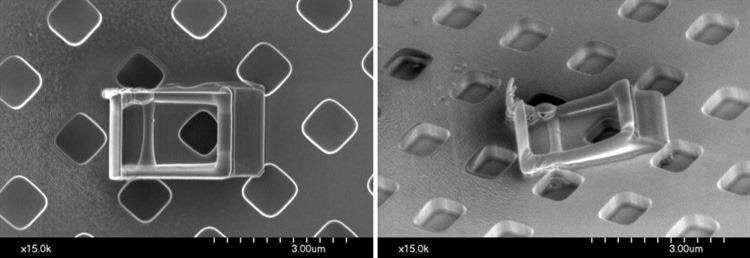
Figure 3. Contamination formed on a silicon wafer sample during 2 hours of continuous electron beam bombardment. The left image was taken with 60° sample tilt and the three-dimensional structure of the contamination can be observed. Image Credit: Evactron (XEI Scientific)
Just before the frame scan was initiated, the electron beam dwelled slightly more at the upper left corner and, therefore, the electron beam remained immobile at that point for the longest time overall and created a considerably taller contamination peak (similar to an e-beam-deposited AFM probe).
The drifting of the electron beam and/or the sample stage during the extended irradiation time seemed to distort the structure.
The existence of the vertical line (initially, the left edge of the frame) proximal to the center of the contamination-induced frame evidently demonstrates that after the contamination has been deposited, the electron beam can no longer eliminate it.
If visualized at high magnification in real time, the operator does not voluntarily observe the contamination.
The image shown on the viewing screen is around 20% smaller than this frame and, therefore, the electron beam typically over-scans a larger region on the specimen than the electron beam shows on the screen.
Hence, the most disturbing aspect of the contamination deposited at high magnification underscores the fact that the contamination effect is generally not observed by the operator except when reverting to lower magnifications.
An etched silicon sample at 50,000 times magnification is shown in Figure 4. This specimen was struck with a 5 kV, 10 pA electron beam at 500,000-fold magnification. The area shown on the SEM screen at this magnification is marked proximal to the middle of the image.
The image at 500,000 times magnification is introduced at the lower right corner. The usual mark of frame-like contamination is no longer visible; the dynamic process created only a circle at this extremely high magnification. The electron beam was left on the specimen for 10 minutes.
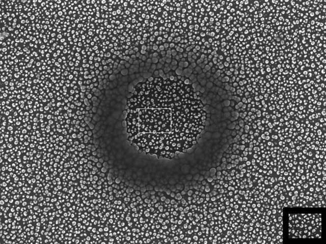
Figure 4. Etched silicon sample at 50,000 times magnification, which was bombarded with a 5 kV, 10 pA electron beam at 500,000 times magnification. Image Credit: Evactron (XEI Scientific)
Two images captured with the CD-SEM are shown in Figure 5. In this example, the (800 V, 3 pA) electron beam strikes the specimen for 6 minutes.
During this period, the sample/beam drift and the contamination causes the enlargement of the corner section by around 0.15 µm. Analogous effects can take place in shorter times and, in extreme cases, even in just a few seconds.
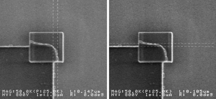
Figure 5. X and Y enlargement of the corner region due to contamination and drift in a CD-SEM. 800 V, 3 pA electron beam bombardment for 6 minutes. Image Credit: Evactron (XEI Scientific)
The extent to which the deposited contamination contributes to measurement inaccuracies in CDSEMs will continue to be vague unless the operator is familiar with this issue and correct and reliable examinations and measurement of the contamination rate are performed.
Anti-Contamination Devices
Evidently, contamination induced by the electron beam is believed to be a major issue in scanning electron microscopy and no system is entirely free of this issue. Even dry pumped instruments can deposit contamination (usually, at a relatively lower rate).
Contamination also occurs from hydrocarbons that are brought close to the electron beam by the sample itself. The extent of the issue could be demonstrated through regular measurements of the contamination rate; however, if the errors caused by contamination are too high, then something needs to be done to mitigate the issue.
The use of a liquid nitrogen anti-contamination device is one possibility with certain SEMs. An anti-contamination device is essentially a compact, flat metal piece mounted above the surface of the sample that is maintained at liquid nitrogen temperatures.
The anti-contamination device, by operating fundamentally as a cold trap or getter pump, gathers a good portion of the contaminants. Therefore, the rate of localized sample contamination at the specimen is decreased.
But it must be noted that the confined contaminants are discharged as soon as the device is allowed to warm up. An etched silicon sample observed at 50,000 times magnification in an instrument, equipped with a liquid nitrogen anti-contamination device, is shown in Figure 6.
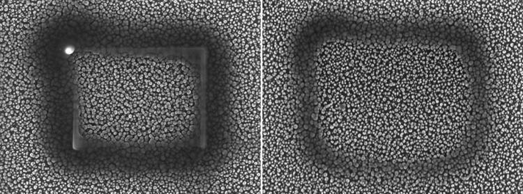
Figure 6. Two locations of a silicon sample irradiated for 10 minutes without (left) and with (right) the application of liquid N2 to cool the anti-contamination device (50,000x). Image Credit: Evactron (XEI Scientific)
This specimen was bombarded twice at two different sites at 100,000 times magnification for a period of 10 minutes (at 5 kV, 10 pA).
In Figure 6, The left image shown was taken without adding liquid nitrogen to the device, and the right image was taken using the same conditions but with the anti-contamination device fully charged with liquid nitrogen. The level of contamination is certainly decreased but it still continues to remain high.
Evactron Cleaning
Figure 7 shows a couple of images of the same silicon specimen visualized in the same SEM as Figure 6. For comparison purposes, the left image is the same as the one on the left of Figure 6; however, the right image was captured after switching on the Evactron unit and applying the cleaning process for 10 minutes.
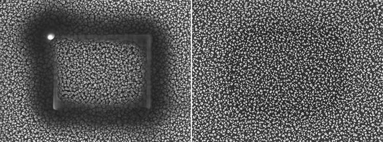
Figure 7. Two locations of a silicon sample irradiated for 10 minutes before (left) and after (right) the use of an Evactron anti-contamination device. 50,000x. Image Credit: Evactron (XEI Scientific)
The level of contamination is considerably decreased on the right side of Figure 7, where the Evactron anti-contamination device was used. Moreover, the amount deposited is much less than even with the liquid nitrogen-cooled anti-contamination device.
The SEM served as a cold-field emission gun instrument that was used to capture the images in Figure 7. This instrument was fitted with a liquid nitrogen cold trap on top of the water-cooled baffle above the diffusion pump. The instrument was also equipped with a gaseous nitrogen leak system in which needle valves in the fore lines of the mechanical pumps are fixed at around 2 Pa.
This deliberately blocks the rotary pumps from achieving their ultimate vacuum (Postek, 1996). This leak is sufficiently small to ensure that the pump efficiently backs the diffusion pump or to pump-down the specimen exchange chamber without affecting the ultimate chamber vacuum.
But the infinite streaming of nitrogen molecules into the line decreases the ability of backstreaming of oil from the rotary pumps. This basic system provides an effective mechanism for reducing contamination induced by the instrument. But in several cases, as demonstrated here, it may not be adequate.
CD-SEMs are often fitted with turbomolecular pumps and oil-free fore-line pumps to offer a better, cleaner vacuum. Even with these kinds of pumps, several SEMs are not sufficiently clean and unwanted contamination deposition eventually occurs.
Constant monitoring and, if required, instrument cleaning should be carried out. Two potential ways can be followed for monitoring:
- Quantify the contamination rate using the Evactron, which shows the cleanliness of the vacuum.
- Quantify the impact on dimensional measurement by determining the change that occurs during recurrent measurements.
Generally, the rate of measurement is more advantageous but it may not be as relevant to all the specimens. This is because different samples composed of different materials tend to contaminate at different rates and the specimens themselves are also the sources of the contaminating molecules.
Another prospect for sample dimensional change that should be considered is that exposure to the electron beam itself can distort the sample under test (Postek et al., 1989). Therefore, it is essential to accurately assess the difference between change caused by contamination deposition and the change induced by the electron beam.
After many Evactron treatments, the vacuum remains clean for extended periods and the frequency of required Evactron treatments becomes less. But since the cleanliness of the vacuum also depends on the nature and cleanliness of specimens going through the system, reliable monitoring of the rate of contamination can indicate when another cleaning cycle should take place.
An image taken with a tilt wafer SEM is shown in Figure 8. Prior to Evactron cleaning, it was not possible to work without considerably contaminating the specimen. The instrument was subjected to a series of 10 minutes of Evactron cleaning.
Post this cleaning, only a small quantity of contamination developed under the electron beam. This was shown by the light mark of contamination on the clean, newly etched polysilicon specimen.
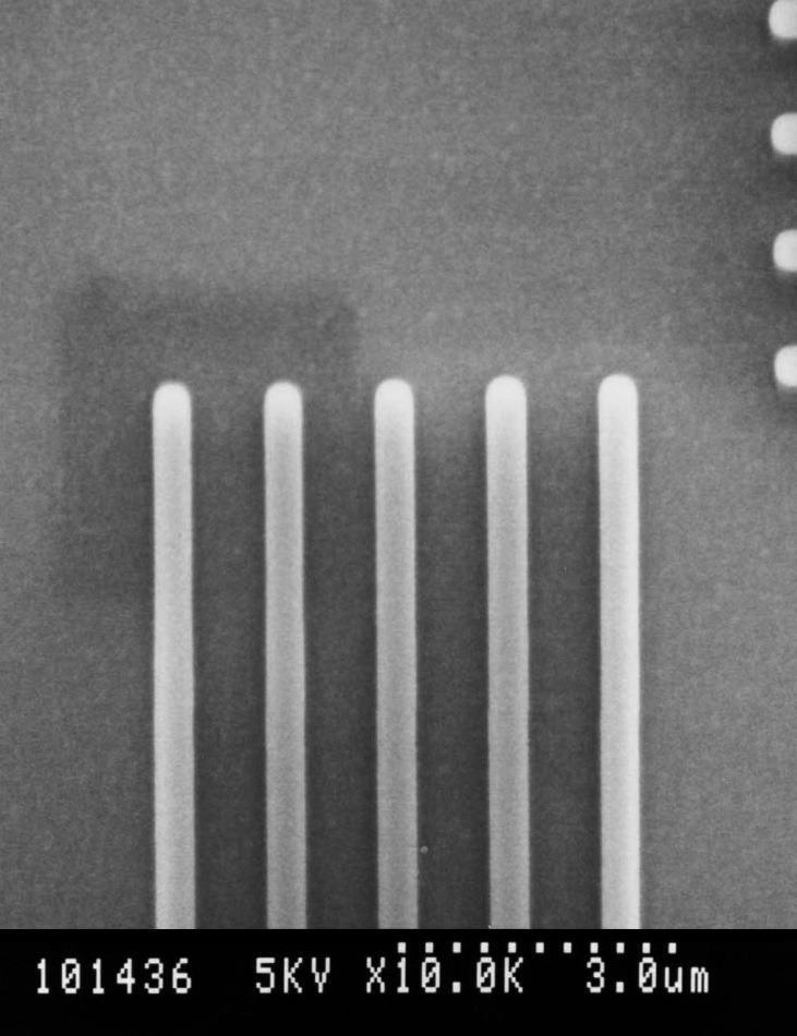
Figure 8. Tilt wafer SEM. Minimal contamination mark on a polysilicon sample after treatment, 15 minutes dwell time at 30,000x magnification, at 5 kV. Image Credit: Evactron (XEI Scientific)
Sample Cleaning
Once contamination has been deposited on a specimen, it can be removed to some extent through in-situ oxygen plasma cleaning by the Evactron. This cleaning process is shown on a silicon specimen in Figure 9.
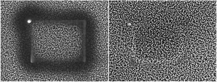
Figure 9. Silicon sample that was irradiated for 10 minutes. The left image was taken after contamination deposition and is shown untreated. The image on the right was taken after a 60-minute in-situ treatment of the sample with Evactron anti-contamination device. 50,000x. Image Credit: Evactron (XEI Scientific)
Both sample locations were irradiated for 10 minutes. The left image shown in Figure 9 is the untreated specimen. The right image in Figure 9 was taken after treating the sample for 60 minutes with the Evactron anti-contamination device. It is important to emphasize that prolonged sample treatment may also change the “clean” areas.
Conclusions
Contamination of varied samples under the electron beam has been demonstrated to cause measurement inaccuracies in laboratories and CD-SEMs. The extent of the error is unknown unless the rate of contamination is steadily monitored. The contaminating molecules should be removed depending on the severity of the issue.
This article has explained a novel cleaning technique using an active plasma system that was found to be effective in decontaminating the vacuum of the specimen chamber of a laboratory as well as production metrology SEMs.
References
- Postek, M. T. 1996. An approach to the reduction of hydrocarbon contamination in the SEM. SCANNING 18:269-274.
- Postek, M. T. 1989. Scanning Electron Microscope-based Metrological Electron Microscope System and New Prototype SEM Magnification Standard. Scanning Microscopy 3(4):1087-1099.
- Reimer, L.: Image Formation in Low-Voltage Electron Microscopy SPIE Opt. Eng. Press; Volume TT 12 (1993) ISBN 0-8194-1206-6.

This information has been sourced, reviewed and adapted from materials provided by XEI Scientific.
For more information on this source, please visit XEI Scientific.