Utilizing FIB-SEM, nanofluidic lab-on-a-chip devices for the analysis of single DNA molecules were characterized and fabricated. Direct FIB nanopatterning of silicon master stamps enables the quick prototyping of nanochannels of different cross-sections, shapes and depths.
In addition, the fabrication of 3D structures, for example, funnel-shaped inlets to connect the nanochannels to the much wider, deeper microchannels, is relatively simple. This is vital to ensure an optimal DNA flow in the fluidic chip.1
The silicon master stamp is transferred to a polymer-on-glass stamp by means of UV nanoimprinting the pattern, which is utilized as a stamp in a second UV nanoimprint step to fabricate the actual chip.
Not only the master stamps can be machined in the FIB-SEM, but the complete fabrication process can also be observed in a non-destructive fashion.
To enable the utilization of the devices after their inspection, ZEISS local charge compensation allows the high-resolution SEM characterization of the highly insulating polymer-on-glass stamps and devices without any metal coating.
In addition to environmental factors and living habits, genes determine our predisposition to suffer from particular diseases. If tailored to the genetics of the patient, the medical treatment of a disease can also be more efficient.
Impressive results have been reported, such as more effective cancer therapies,2,3 the cure of genetic diseases4 and disease prevention by lifestyle changes,5 despite this new field of personalized medicine still being in an experimental phase.
These advances demonstrate that personalized medicine can revolutionize healthcare if affordable, quick DNA screening can be realized. Sequencing techniques have developed dramatically in the last decade. Yet, they are still too expensive and slow to make personalized therapies accessible to the public.
Optical mapping is one promising alternative for simple, quick and affordable analysis of single DNA molecules.6 This technique can benefit from nanofluidic chips created using UV-nanoimprint lithography (UV-NIL).7,8
These devices possess nanochannels, where the DNA molecules can be stretched and observed for analysis. This research work created the nanochannels of silicon master stamps using focused ion beam (FIB) direct lithography with ZEISS Crossbeam 550.
The subsequent, different byproducts of the UV-NIL process could be characterized by high-resolution scanning electron microscopy (SEM) by utilizing this same instrument. A local charge compensation method was employed for the imaging of insulating materials.
Master Stamp Fabrication by FIB
An SEM image of a master stamp after FIB nanopatterning can be seen in Figure 1.
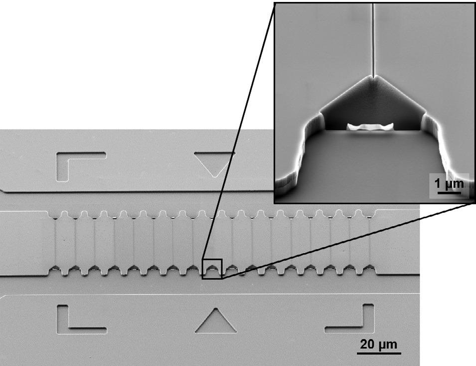
Figure 1. SEM image of a silicon master stamp with straight nanochannels after FIB patterning. The inset shows the tapered nanochannel inlet. The sample is tilted 54°. Image Credit: Carl Zeiss Microscopy GmbH
The master stamp is made of silicon and the micron-sized fluidic structures (with dimensions of 15 µm and over) were patterned using photolithography and reactive ion etching.
FIB was used to pattern much narrower channels directly into the silicon master stamp. These nanochannels are under 100 nm wide and 38 µm long, and they connect top and bottom microchannels.
Whole molecules or fragments of DNA are driven through the narrow channels by electrophoresis in the optical mapping experiment, for example, by applying an electric potential difference between the microchannels.
As DNA has a net charge, it is driven into the nanochannels to pass from one microchannel to the other. The DNA molecules are uncoiled and elongated inside the nanochannels, which enables the optical mapping measurement.9
As seen in the image, the funnel-shaped inlet facilitates the threading and pre-stretching of the DNA into the channel.1
These 3D structures can be easily fabricated by using FIB direct lithography with the right choice of parameters. This is a key benefit for this application compared to other possible nanopatterning methods. Another benefit of FIB direct patterning is that it enables fast prototyping.
The layout of the nanochannels can be easily tailored to match the requirements of the experiment because of this. For instance, Figure 2 demonstrates meander channels with a total length of almost 200 µm for the analysis of larger DNA fragments. As a result of FIB milling dose variation, the channel width decreases from left to right.
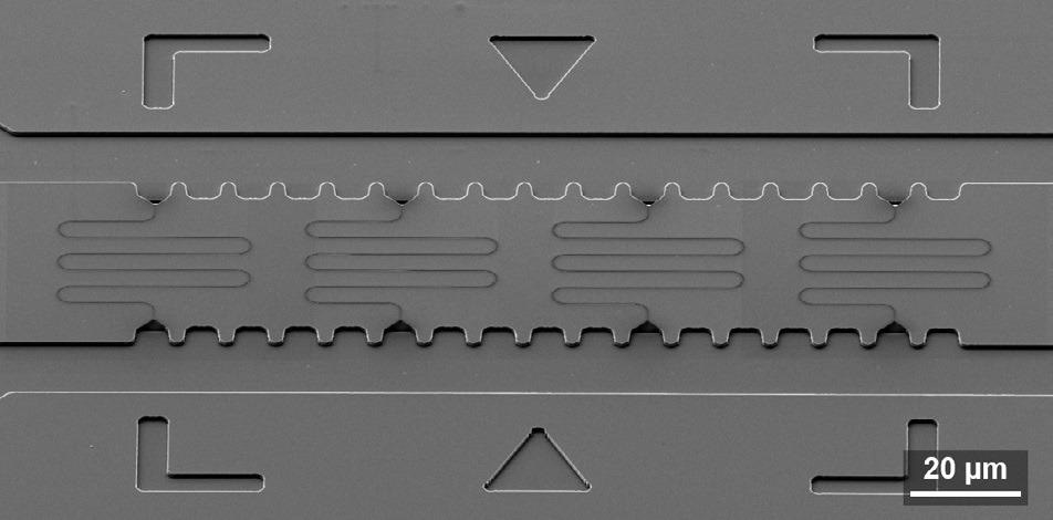
Figure 2. SEM image of a silicon master stamp with meander nanochannels. The sample is tilted 54°. Image Credit: Carl Zeiss Microscopy GmbH
Direct control of the nanochannel FIB milling was possible using ZEISS Crossbeam’s live SEM imaging at the instrument’s best resolution.10 Therefore, milling recipes could be efficiently optimized.
Process Control with Charge Compensation
As seen in Figure 3, the actual devices for the DNA optical mapping experiment are fabricated by using two-step UV-NIL.7,8
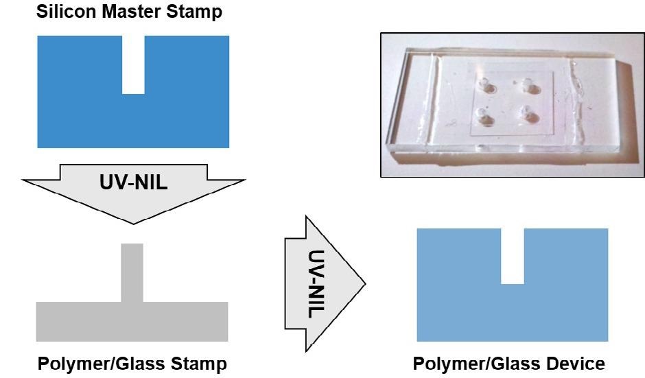
Figure 3. Schematic of the two-step UV-NIL process for the mass fabrication of devices for DNA optical mapping. Image Credit: Carl Zeiss Microscopy GmbH
In a first step, the FIB fabricated silicon master stamp is imprinted into a polymer layer on a glass substrate, the polymer-on-glass stamp. In a second step, the polymer-on-glass stamp is replicated again in the same polymer-on-glass system.
So, the original geometry of the silicon master stamp is recovered on the final device after the two steps. Both the polymer-on-glass stamp and the master stamp can be reused, making the method suitable for cheap mass production of nanofluidic chips.
The polymer-on-glass system is difficult to image, while SEM characterization of the silicon master stamp is straightforward. Figure 4a demonstrates the polymer-on-glass device imaged at 1.31 keV electron landing energy.
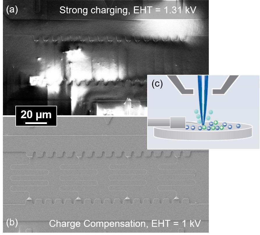
Figure 4. SEM images of a polymer-on-glass stamp without (a) and with charge compensation (b). The inset (c) shows the principle of local charge compensation. Image Credit: Carl Zeiss Microscopy GmbH
Severe charging of the polymer-on-glass stamps and samples was observed in the SEM and even for low primary beam energies and currents.
These samples, therefore, were studied utilizing local charge compensation. This is a charge neutralization option that is available on ZEISS electron microscopes.
Put simply, a gas injection needle is placed near the sample and dry nitrogen injected through the needle, as seen in Figure 4c. The primary beam ionizes the gas, and the ions neutralize any excess charge built up in the sample in a self-sustaining manner.
The rise in chamber pressure is under 10-2 mbar as the nitrogen injection is local, and so Inlens SE detection is still possible. Furthermore, the short gas path length minimizes detrimental scattering effects. The result is a clear and crisp SEM image which can be seen in Figure 4b.
With local charge compensation, the polymer-on-glass stamp could be compared with the corresponding original structure in silicon, and an example can be seen in Figure 5. The polymer-on-glass stamp could be reused in later experiments as it was not coated for SEM observation.
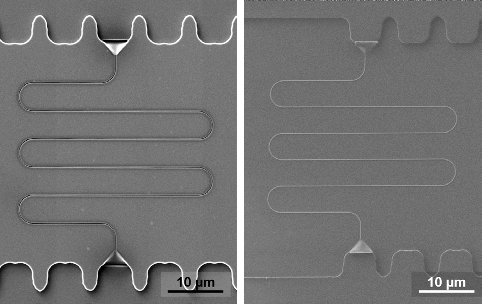
Figure 5. SEM images of a silicon master stamp with a meander nanochannel (left) and the same structure in the corresponding polymer-on-glass stamp (right). Image Credit: Carl Zeiss Microscopy GmbH
Local charge compensation on the polymer-on-glass samples was very efficient. Crucial details of the nanochannels could be studied with high resolution, as seen in Figure 6, especially the continuity and profile of the nanochannel and the 3D shape of its two inlets.
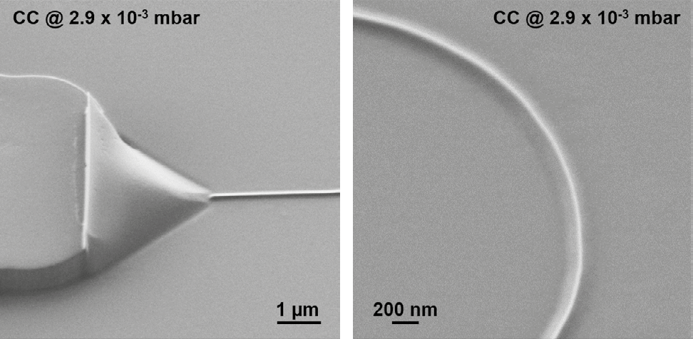
Figure 6. Close-up images of the inlet (left) and bend (right) of a polymer nanochannel using local charge compensation. Image Credit: Carl Zeiss Microscopy GmbH
Conclusion
In the field of nanofluidics and single molecule detection, ZEISS Crossbeam is a very useful tool for research. The application described in this article is a good example.
On the one hand, FIB direct lithography allowed fast and flexible prototyping of the finest nanoscale structures in the silicon master stamps, including 3D shapes. On the other hand, SEM with the same instrument enabled the optimizing and monitoring of the entire nanoimprint process without interfering with it.
There was no need to sputter coat the insulating polymer-on-glass stamps with local charge compensation, and they could be reused after their quality assurance.
Acknowledgments
Produced from materials originally authored by Parisa Bayat, Robert H. Blick, Irene Fernández-Cuesta from Center for Hybrid Nanostructures (CHyN), University of Hamburg and Fabián Pérez-Willard, Tobias Volkenandt from Carl Zeiss Microscopy GmbH.
References
- F.M. Esmek et al., Sculpturing wafer-scale nanofluidic devices for DNA single molecule analysis, Nanoscale 11 (2019), pp. 13620-13631.
- I.I. Wistuba et al., Methodological and practical challenges for personalized cancer therapies, Nat. Rev. Clin. Oncol. 8 (2011), pp. 135-141.
- T. Tursz et al., Implications of personalized medicine – perspective from a cancer center, Nat. Rev. Clin. Oncol. 8 (2011), pp. 177–183.
- R.E. MacLaren et al., Retinal gene therapy in patients with choroideremia: initial findings from a phase 1/2 clinical trial, Lancet 383 (2014), pp. 1129-1137.
- L. Hood and S.H. Friend, Predictive, personalized, preventive, participatory (P4) cancer medicine. Nat. Rev. Clin. Oncol., 8 (2011), pp. 184-187.
- E.T. Lam et al., Genome mapping on nanochannel arrays for structural variation analysis and sequence assembly, Nat. Biotechnol. 30 (2012), pp. 771-776.
- I. Fernandez-Cuesta et al., Fabrication of fluidic devices with 30 nm nanochannels by direct imprinting, J. Vac. Sci. Technol. B29 (2011), 06F801-1/7.
- I. Fernandez-Cuesta et al., A nanochannel through a plasmonic antenna gap: an integrated device for single particle counting, Lab Chip 19 (2019), pp. 2394-2403.
- C. Freitag et al., Visualizing the entire DNA from a chromosome in a single frame, Biomicrofluidics 9 (2015), p. 044114.
- T. Volkenandt and F. Pérez-Willard, Enabling smart FIB work with SmartSEM, ZEISS Technology Note (2016).

This information has been sourced, reviewed and adapted from materials provided by Carl Zeiss Microscopy GmbH.
For more information on this source, please visit Carl Zeiss Microscopy GmbH.