Graphene is now the most well-known 2D material. It is comprised of a sheet of covalently bonded carbon atoms arranged in a hexagonal lattice where the thickness has been broken down to a single atom.
This novel nanomaterial is exceptionally strong and possesses the greatest known thermal and electrical conductivity. Andre Geim and Konstantin Novoselov were granted the Nobel prize for Physics in 2010 for their graphene research.
Other 2D materials are also actively being explored. Xenes are a collective group of graphene-like structures that are also monolayers of a single element.
For instance, as a potential material for transistors, single-layer black phosphorus – phosphorene – offers much promise. Other examples are silicene (silicon), germanene (germanium) and stanine (tin), all of which demonstrate a hexagonal structure like graphene with various degrees of buckling.
The overall structure of hexagonal boron nitride (h-BN) is the same as graphene but substitutes the carbon atoms for varying boron and nitrogen atoms.
Finally, another well-accepted class of 2D materials is transition metal dichalcogenides with the chemical formula MX2 – where M is a transition metal such as tungsten or molybdenum, and X is a chalcogen, such as Sulphur, selenium or tellurium.
Recently there has been a huge amount of interest in graphene as well as other 2D materials. An angular or lattice mismatch has demonstrated the ability to produce different electrical properties of the layered stack.
This paves the way to creating new devices in a bottom-up approach, stacking multiple layers of 2D materials under such angles that facilitate the tuning of the properties.
However, as relaxation processes occur after deposition, control measurements are required to confirm the angular mismatch between the layers.
Why AFM?
AFM has become the preferred instrument for the study of nanomaterials for two primary reasons: resolution, and availability of several modes that enable detailed characterization of a nanomaterial, including its electrical and mechanical properties beyond the topography.
The exceptional x-, y- and z-resolution is crucial due to phenomena close to the atomic scale. The resolution of a commercial AFM laterally extends from less than a few nanometers all the way to atomic resolution and upwards of 0.1 nm vertically.
This makes AFM one of the limited types of instruments that can acquire the resolution needed to determine nanosheets that are just a few angstroms thick.
An additional benefit of AFM that has real-world implications is the suite of measurement modes available to simultaneously evaluate electrical and mechanical properties as well as the topography.
These modes can be applied to investigate those supplementary properties in detail or simply as a contrast mechanism to assess the quality of grown graphene or any angular mismatch between stacked layers of graphene.
This makes AFM an essential tool for designing devices that are contingent on the stacking of 2D materials.
Lastly, the AFM tip can be used for sample manipulation at the nanoscale. However, graphene can, for instance, be applied to cut through graphene sheets.
The two halves of a single graphene sheet cut in two possess the same crystal orientation, improving the control of the angular mismatch during stacking.
Besides these imaging properties, a further incentive for the application of AFM stems from its compact footprint, allowing it to be placed inside a glovebox. This is a key requirement for the study of graphene in combination with 2D materials that are sensitive to the presence of humidity or oxygen.
Applications
Examples of AFM’s strength for the characterization of graphene are demonstrated in the following applications.
Flake Thickness
The first example demonstrates the outstanding resolution of AFM. Figure 1 exhibits a number of stacked layers of graphene oxide, facilitating the analysis of the thicknesses of the individual layers.
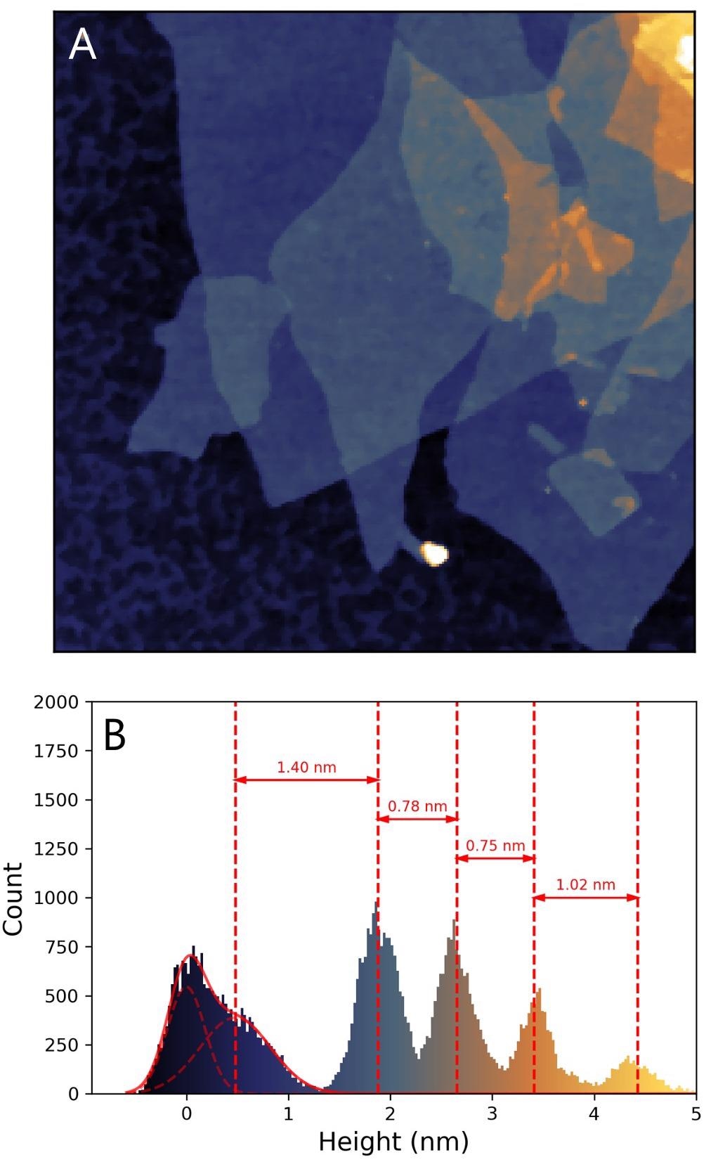
Figure 1. Measuring the thickness of multilayer graphene. (A) AFM topographical image of graphene oxide with lateral dimensions of 5.11 x 5.11 µm2. (B) Histogram of the heights in (A) showing the thickness of the first 4 layers. Image Credit: Nanosurf AG
A comparable height histogram of the measurement reveals that the thinnest layer is a mere 0.75 nm. This image shows the excellent vertical resolution of AFM at the level necessary for the evaluation of 2D materials.
Graphene Growth Analysis
An example of the capability to review the quality of graphene is displayed in Figure 2. The sample is comprised of graphene grown by chemical vapor deposition (CVD) on copper.
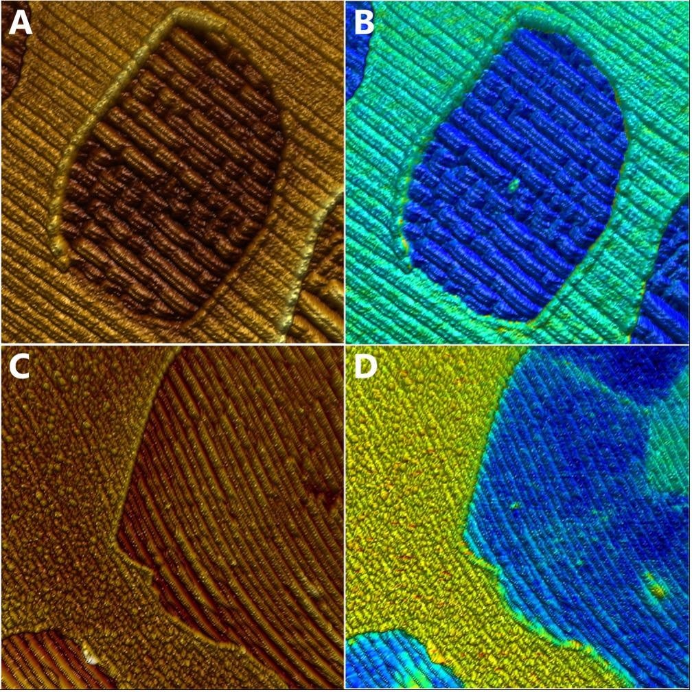
Figure 2. Quality control of CVD grown graphene on post-oxidized copper by lateral force imaging and KPFM. (A) Topography and (B) friction force images, simultaneously recorded. The friction was calculated from the difference between the forward and backward lateral deflection channels. Scan size: 5 x 5 µm2. (C) Topography and (D) contact potential difference images. Scan size 10 x 10 µm2. Image Credit: Nanosurf AG
The copper substrate is not atomically flat, which at times obscures the edges and fine features of the flakes. The copper was oxidized after the deposition, which resulted in the height of the oxidized copper surpassing that of the graphene flake in the topography (Figures 2A and 2C).
The lateral force image (Figure 2B) presents lower friction on the graphene (blue contrast) in contrast with the copper substrate (green contrast) that supports a review of the graphene coverage of the copper substrate, considering that the edges possess a sharper contrast in the friction channel than in the topography.
Additionally, the friction image clearly demonstrates higher friction in the center of the flake, presenting the growth seed point of the flake that cannot be seen in the topography.
Kelvin probe force microscopy (KPFM) was also used for the analysis of this sample (Figure 2D). Traditionally, KPFM is applied in the analysis of contact potential difference (CPD) between tip and sample, and under vacuum conditions even the work function.
As anticipated, graphene and the oxidized copper exhibit a different CPD, with graphene possessing a lower value.
Crucially, the CPD image presents a heterogeneity on the graphene, with some fine lines and areas on the graphene flakes that are not discernable in the topography, thus improving the quality assessment of the graphene deposition process by AFM.
Lattice Mismatch
The AFM tip and a graphene layer interaction are also contingent on the interaction of the graphene layer with the layer below. Where an angular mismatch is present, the interaction periodically varies with a lattice constant subject to the angular mismatch.
This regular pattern, also known as moiré super lattice, can be visualized with the application of AFM, for instance, by piezo-response force microscopy (PFM)1 or force modulation,2 oscillating the cantilever at the contact resonance frequency.
A cantilever with sample contact via the tip has different resonances than a free-swinging cantilever. The first contact resonance is extremely sensitive to the sample’s mechanical properties.
Measurement of the contact resonance can be conducted directly using a phase-locked loop or dual frequency resonance tracking, or indirectly but more efficiently by identifying the phase and amplitude via the excited cantilever at a fixed frequency on the contact resonance peak.
This contact resonance frequency can be established from a thermal tune spectrum as reported by the tip in contact with the sample.
The angular disparity between two layers of graphene can be determined from the periodicity of the moiré superlattice.
Figure 3 displays the phase and amplitude response acquired by imaging a double layer of twisted graphene, clearly displaying the moiré pattern resulting from an angular mismatch.
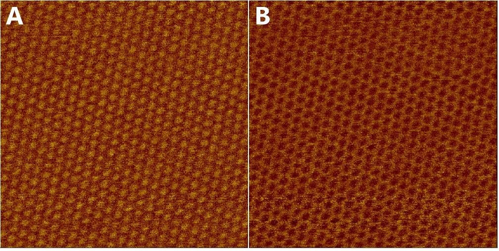
Figure 3. Moiré super lattice of twisted graphene on hBN imaged in PFM mode at the contact resonance frequency. (A) amplitude and (B) phase. Scan size: 154 x 154 nm2. Sample courtesy: Nanoelectronics group TIFR, India. Image Credit: Nanosurf AG
Electro-static excitation of the cantilever was performed in PFM mode at the contact resonance frequency. Predicated on the lattice constant of the moiré pattern, the angular mismatch of this sample came to 2.2°.
Figure 4 demonstrates the phase response measured in force modulation imaging mode on a DriveAFM.2 In this instance, photothermal excitation of the cantilever was conducted on the contact resonance peak.
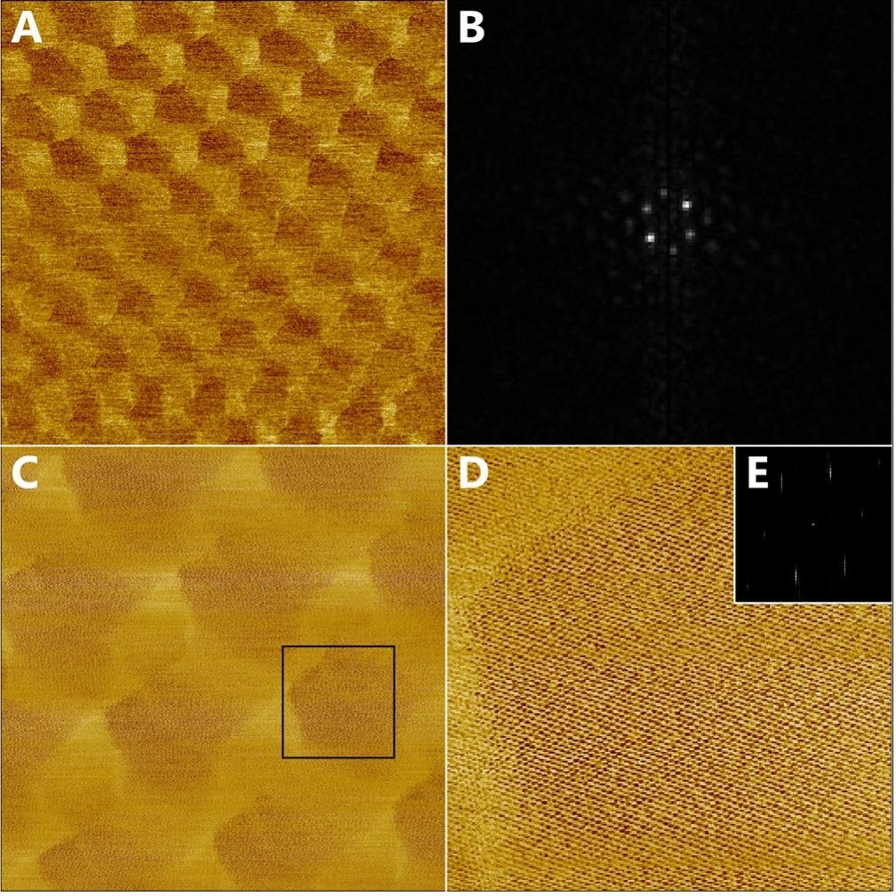
Figure 4. Moiré super lattice of twisted graphene on hBN imaged in force modulation mode on the contact resonance frequency. (A) phase image with scan size of: 190 x 190 nm2 (B) Center part of the Fourier transform image used to determine the lattice constant of the moiré pattern (C) phase image of 68 x 68 nm2 area rescanned with 1024 x 1024 px2 containing both the moiré superlattice and atomic lattice. (D) Digital zoom of the (C) of 17 x 17 nm2. (E) Fourier transform showing the diffraction spots from the atomic lattice. Image Credit: Nanosurf AG
The 192 nm wide image of Figure 4A exhibits a lattice with some extent of distortion, signaling a variation in the angular mismatch but still providing multiple diffraction spots in frequency space after Fourier transformation (Figure 4B).
The frequency of 1/(7.26 nm) of the (2;2) diffraction spot close to the fast scan axis can be transposed to a lattice constant of 29 nm in real space.
This is 117 times greater than the lattice constant of graphene, depicting an angular mismatch close to 0.5°. Recording a 68 nm wide image (C) with 1024 x 1024 px2 shows the atomic lattice in addition to the moiré super lattice.
A digital zoom of 17 nm in width of the phase signal is presented in Figure 4D to improve the visibility of the lattice in real space, and Figure 4E exhibits the Fourier transform of the phase signal. In order to confirm the lattice of the moiré super lattice, the atomic lattice was applied.
Cutting Graphene
As previously mentioned, the AFM tip can be applied to manipulate as well as to measure materials on the nanometer scale. Figure 5 displays an example of a multi-layer stack of graphene that used an AFM tip to cut in nano-lithography mode. The experiment was conducted on a FlexAFM.
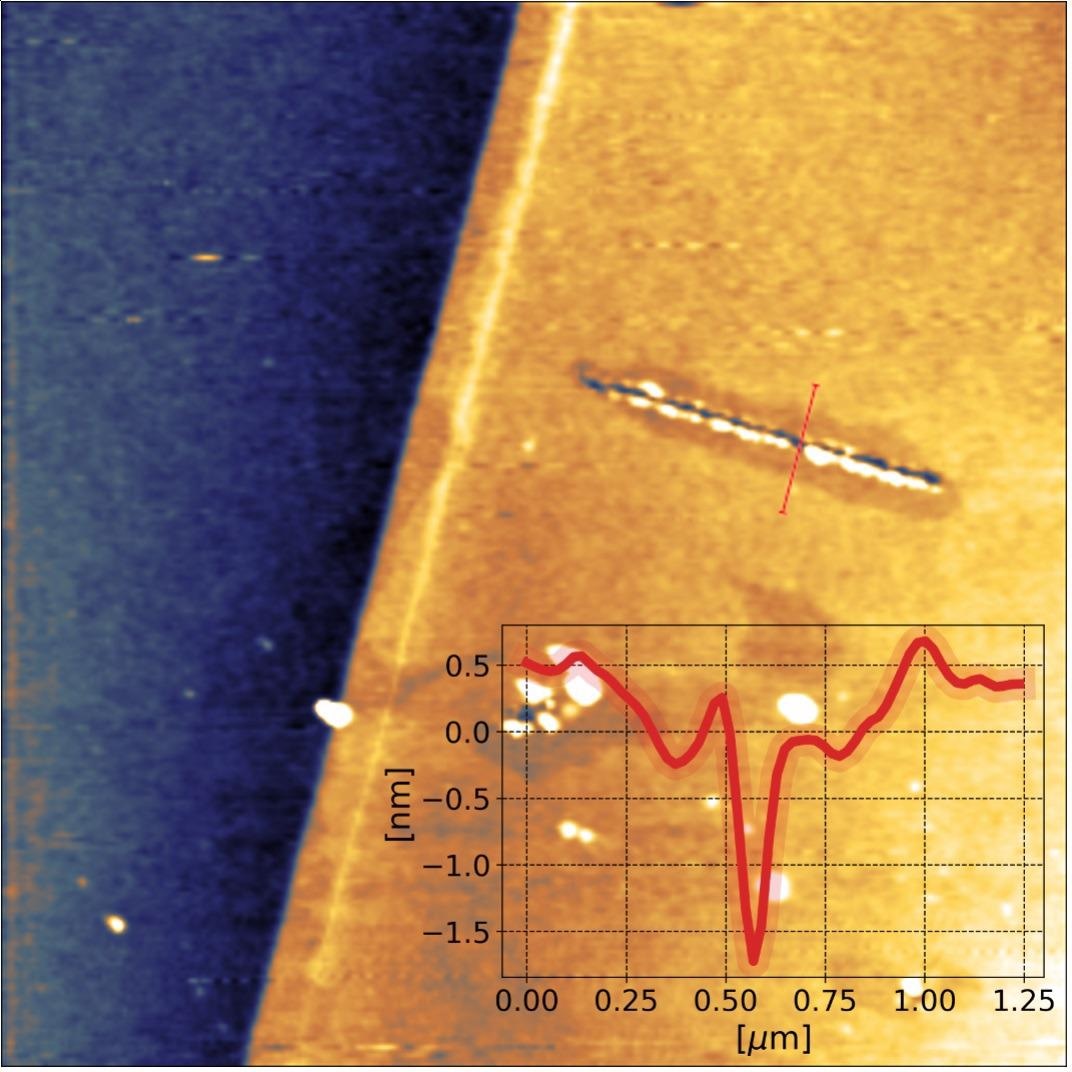
Figure 5. Cutting graphene by AFM lithography. AFM topography image of a multilayer graphene flake on Si substrate with lateral dimensions of 10 x 10 µm2. Cuts were obtained by applying a 10V AC voltage at 500 kHz to the tip of a BudgetSensors ElectriTap190E cantilever (k = 48 N/m nominal) and following the designated path in Static Force Mode with an applied force of 5 µN at a speed of 100 nm/s. The relative humidity was 42%. Sample courtesy: Kim group, Harvard University, USA. Image Credit: Nanosurf AG
In lithography, control over the cutting process can be determined by a number of parameters, such as force, speed and direction. At the same time, applying a DC or AC voltage or combination of both between tip and sample may influence the depth of the cut. It is presumed that the cutting mechanism takes place through local anodic oxidation of the surface.3-5
The high voltages around the tip dissociate H2O into H and OH groups, which oxidize the graphene. The graphene is then fractured by the tip-induced mechanical stress at the locations it was oxidized.
For this reason, the relative humidity surrounding the tip plays a key role in the cutting of graphene. The environmental control add-on facilitates accurate close-control of the humidity surrounding the samples.
Conclusion
2D materials like graphene or xenes – or transition metal dichalcogenides – are a rapidly-growing topic of interest among leading nanomaterials researchers, with promising applications in transistors, sensors and optoelectronics.
AFM is well-suited for the investigation of such materials owing to its excellent resolution well below a nanometer, with the capacity to clearly show the atomic lattice and atomic steps.
As a characterization tool, AFM can perform many functions, such as measuring and correlating a number of key properties of these materials to better comprehend and characterize them.
The detection of moiré patterns is one such example of this type of characterization. In addition, AFM can be applied to locally manipulate 2D materials.
To sum up, AFM is an indispensable tool for the study of graphene and other 2D materials in pursuit of optimizing integration into devices and other applications.
References
- McGilly et al 2020 Nat. Nanotechnol. 15, 580–584
- Adams et al 2021 Rev. Sci. Instr. 92, 129503
- Puddy et al 2011, Appl. Phys. Lett. 98, 133120
- Masubuchi et al 2011, Nano Lett. 11, 4542–4546
- Li et al 2018, Nano Lett. 18, 8011-8015

This information has been sourced, reviewed and adapted from materials provided by Nanosurf AG.
For more information on this source, please visit Nanosurf AG.